ChipApex | Global Electronic Components Supplier

SEARCH
Search Product
Search Post
— IC芯片 | 连接器 | 传感器 | 被动器件 —
Search productSearch post
— IC芯片 | 连接器 | 传感器 | 被动器件 —
Consult the customer manager about the wholesale price.
consultation hotline:86-132-6715-2157
email:[email protected]
Contact the product manager for consultation. One-stop consultation is available.
Do you want a lower wholesale price? Please send us your inquiry and we will reply immediately.
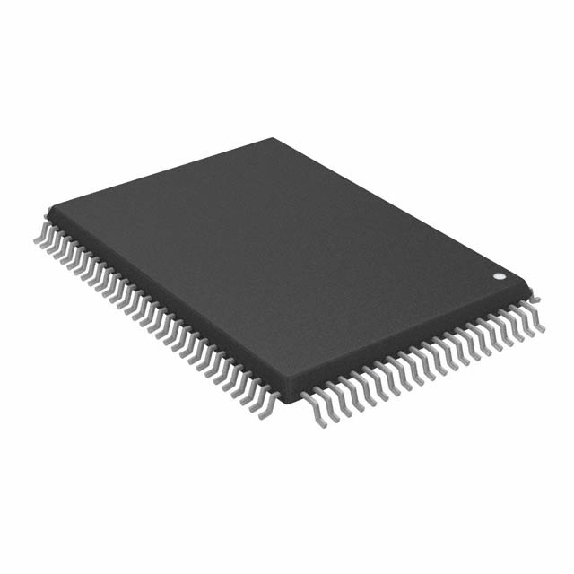
CY7C1440KV33-250AXC is listed in the Memory IC range at ChipApex. The manufacturer field lists Cypress Semiconductor Corp. Its product description is IC SRAM 36MBIT PAR 100TQFP. Review the specifications below when checking this part for your BOM.
The CY7C1440KV33-250AXC is a 36-Mbit (1M × 36) Pipelined Synchronous SRAM featuring on-chip ECC. It supports bus operations up to 250 MHz with a maximum clock-to-output time of 2.5 ns. The device utilizes registered inputs and outputs for pipelined operation, providing a high-performance 3-1-1-1 access rate. It operates from a 3.3 V core power supply with 2.5 V or 3.3 V I/O options. Key features include user-selectable burst sequences, separate processor and controller address strobes, synchronous self-timed writes, and an asynchronous output enable.
Verify the specific speed grade and package type against the datasheet ordering information. Confirm that the ECC functionality is required, as non-ECC variants exist within the same family. Ensure voltage levels match the 3.3 V core and 2.5/3.3 V I/O specifications. Check for availability of the 100-pin TQFP or 165-ball FBGA packages depending on design constraints.
Select this component when single-bit error correction is critical for system reliability. Choose the 250 MHz grade for maximum throughput requirements. Consider the 1M × 36 organization for wide data path applications. Verify compatibility with the target processor's burst sequence requirements (interleaved vs. linear). Ensure the PCB layout supports the selected package type and JTAG interface if boundary scan testing is needed.
This part belongs to the Cypress CY7C1440KV33/CY7C1442KV33/CY7C1440KVE33 family of 36-Mbit Pipelined Sync SRAMs. It shares architectural similarities with other members like the CY7C1442KV33 but differs in data width and ECC implementation. The family is designed for high-speed synchronous memory applications requiring robust data integrity and flexible burst modes.
CY7C1442KV33-250AXC offers similar performance but with a 2M x 18 organization and no ECC. CY7C1440KVE33 provides the same 1M x 36 organization with ECC but may have different packaging or speed grades. Verify electrical characteristics and pin compatibility before substitution.
The on-chip ECC algorithm detects and corrects all single-bit memory errors, including those induced by cosmic rays or alpha particles, significantly reducing the soft error rate.
The device supports both interleaved and linear burst sequences, which are user-selectable via the MODE input pin.
Yes, the JTAG feature can be disabled by tying the TCK pin LOW to prevent clocking of the TAP controller.
Explore related parts through Memory, Integrated Circuits (ICs), all product categories, ChipApex homepage.
 CY7C1440KV33-250AXC

CY7C1440KV33-250AXC is listed in the Memory IC range at ChipApex. The manufacturer field lists Cypress Semiconductor Corp. Its product description is IC SRAM 36MBIT…
Read More
Choose logic inverter ICs by thresholds, supply, output drive and delay. Compare standard and Schmitt-trigger inputs, power sequencing and replacement checks.
Read More
CY7C1440KV33-250AXC is listed in the Memory IC range at ChipApex. The manufacturer field lists Cypress Semiconductor Corp. Its product description is IC SRAM 36MBIT…
Read More
CY7C1440KV33-250AXC is listed in the Memory IC range at ChipApex. The manufacturer field lists Cypress Semiconductor Corp. Its product description is IC SRAM 36MBIT…
Read More
Understand RF attenuator dB values, fixed and programmable types, impedance, power limits and noise tradeoffs before choosing parts for an RF signal path.
Read More
CY7C1440KV33-250AXC is listed in the Memory IC range at ChipApex. The manufacturer field lists Cypress Semiconductor Corp. Its product description is IC SRAM 36MBIT…
Read More
Select a bridge rectifier by reverse voltage, capacitor charging current, startup surge and cooling. Work through a stated DC voltage and ripple example.
Read More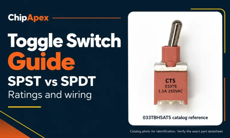
Compare SPST and SPDT toggle switches, understand AC/DC ratings, and follow wiring examples. Check contact action, mounting and parts in the ChipApex catalog.
Read More
CY7C1440KV33-250AXC is listed in the Memory IC range at ChipApex. The manufacturer field lists Cypress Semiconductor Corp. Its product description is IC SRAM 36MBIT…
Read More
Learn how rectifiers convert AC to DC, compare half-wave and bridge circuits, and select voltage, current, recovery and thermal ratings for your design.
Read More
See how a MEMS gyroscope measures angular rate, why its angle estimate drifts, and which range, noise, interface and temperature specs to compare.
Read More
Learn how a pressure transducer converts pressure into voltage, current, or digital output, and compare pressure references and key selection specs.
Read More
The activity of extra discounts on wholesale prices is in full swing…
Please fill in your contact information and we will send you the latest wholesale price list.