 ChipApex | Global Electronic Components Supplier

SEARCH
Search Product
Search Post
— IC芯片 | 连接器 | 传感器 | 被动器件 —
Search productSearch post
— IC芯片 | 连接器 | 传感器 | 被动器件 —
Consult the customer manager about the wholesale price.
consultation hotline:86-132-6715-2157
email:[email protected]
Contact the product manager for consultation. One-stop consultation is available.
Do you want a lower wholesale price? Please send us your inquiry and we will reply immediately.
CY7C1625KV18-333BZXC is listed in the Memory IC range at ChipApex. The manufacturer field lists Cypress Semiconductor Corp. Its product description is IC SRAM 144MBIT PAR 165FBGA. Review the specifications below when checking this part for your BOM.
The CY7C1625KV18 is a 144-Mbit QDR II SRAM organized as 16M x 9. It features separate independent read and write data ports supporting concurrent transactions. The device operates with a maximum clock frequency of 360 MHz, enabling double data rate (DDR) interfaces on both ports for data transfer at 720 MHz. It utilizes two input clocks (K and K) for precise DDR timing and includes echo clocks (CQ and CQ) to simplify data capture in high-speed systems. The memory array uses a single multiplexed address input bus latched for both read and write operations.
Verify that the specific ordering suffix matches the required package type and lead-free status, as Infineon continues to support existing part numbers from the original Cypress development. Confirm supply continuity within the Infineon portfolio, noting that document content remains unchanged despite the corporate transition. Ensure compatibility with existing design-in documentation referencing the original Cypress branding.
Select this component for applications requiring independent read and write ports to eliminate data bus turnaround delays. The CY7C1625KV18 offers a 16M x 9 organization suitable for width expansion or specific word-length requirements compared to the 8M x 18 or 4M x 36 variants. Consider the 360 MHz maximum operating frequency when designing clock distribution networks to ensure signal integrity across the 165-ball FBGA package.
This device belongs to the CY7C16xxKV18 family of 144-Mbit QDR II SRAMs developed by Cypress Semiconductor and now offered by Infineon Technologies. The family includes the CY7C1612KV18 (8M x 18) and CY7C1614KV18 (4M x 36), sharing identical pinouts and functional architectures. All variants utilize the same 165-ball fine-pitch ball grid array package and support similar voltage and timing specifications.
CY7C1612KV18-360BZXC
When the DOFF pin is asserted high, the device operates with a 1.5-cycle read latency. When DOFF is asserted low or connected to ground, the PLL is disabled, and the device behaves in QDR I mode with a 1-cycle read latency.
The ZQ pin is used for output impedance matching. An external resistor (RQ) connects between ZQ and ground to tune the device outputs to the system data bus impedance, typically set to 0.2 times the line impedance.
Explore related parts through Memory, Integrated Circuits (ICs), all product categories, ChipApex homepage.
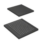 CY7C1625KV18-333BZXC

Learn what an IMU measures, how accelerometers and gyroscopes work together, why orientation estimates drift, and what to compare.
Read More
CY7C1625KV18-333BZXC is listed in the Memory IC range at ChipApex. The manufacturer field lists Cypress Semiconductor Corp. Its product description is IC SRAM 144MBIT…
Read More
Choose a DIP switch by contact type, coded positions, footprint and signal ratings. Check logic polarity, assembly conditions and PCB configuration behavior.
Read More
CY7C1625KV18-333BZXC is listed in the Memory IC range at ChipApex. The manufacturer field lists Cypress Semiconductor Corp. Its product description is IC SRAM 144MBIT…
Read More
Choose logic inverter ICs by thresholds, supply, output drive and delay. Compare standard and Schmitt-trigger inputs, power sequencing and replacement checks.
Read More
Compare RC, crystal and MEMS oscillator circuits. Check ppm, jitter, load capacitance, startup margin and output compatibility before choosing a clock source.
Read More
CY7C1625KV18-333BZXC is listed in the Memory IC range at ChipApex. The manufacturer field lists Cypress Semiconductor Corp. Its product description is IC SRAM 144MBIT…
Read More
CY7C1625KV18-333BZXC is listed in the Memory IC range at ChipApex. The manufacturer field lists Cypress Semiconductor Corp. Its product description is IC SRAM 144MBIT…
Read More
CY7C1625KV18-333BZXC is listed in the Memory IC range at ChipApex. The manufacturer field lists Cypress Semiconductor Corp. Its product description is IC SRAM 144MBIT…
Read More
CY7C1625KV18-333BZXC is listed in the Memory IC range at ChipApex. The manufacturer field lists Cypress Semiconductor Corp. Its product description is IC SRAM 144MBIT…
Read More
CY7C1625KV18-333BZXC is listed in the Memory IC range at ChipApex. The manufacturer field lists Cypress Semiconductor Corp. Its product description is IC SRAM 144MBIT…
Read More
CY7C1625KV18-333BZXC is listed in the Memory IC range at ChipApex. The manufacturer field lists Cypress Semiconductor Corp. Its product description is IC SRAM 144MBIT…
Read More
The activity of extra discounts on wholesale prices is in full swing…
Please fill in your contact information and we will send you the latest wholesale price list.





