 ChipApex | Global Electronic Components Supplier
DG407BDN-T1
Search Product
Search Post
— IC芯片 | 连接器 | 传感器 | 被动器件 —
Search productSearch post
— IC芯片 | 连接器 | 传感器 | 被动器件 —
Consult the customer manager about the wholesale price.
consultation hotline:86-132-6715-2157
email:[email protected]
Contact the product manager for consultation. One-stop consultation is available.
Do you want a lower wholesale price? Please send us your inquiry and we will reply immediately.
The DG407BDN-T1 is a dual 8-channel high-performance CMOS analog multiplexer manufactured by Vishay Siliconix. It selects one of eight differential inputs to a common differential output using a 4-bit binary address. The device operates within a temperature range of -40 °C to +85 °C and utilizes a 28-pin PLCC package. Key electrical specifications include a maximum on-resistance of 74 Ω, a transition time of up to 161 ns, and an off-isolation of -86 dB at 1 MHz. It supports single supply voltages from 5 V to 40 V or dual supplies from ±5 V to ±20 V.
Verify that the specific part number matches the required package type and suffixes. Confirm RoHS compliance status if lead-free terminations are mandatory for the assembly process. Ensure the ordering quantity aligns with the manufacturer's tape and reel packaging requirements.
Select this component when differential signal routing is required in a compact form factor. Verify that the maximum supply voltage does not exceed 44 V between rails. Check that the charge injection and on-resistance values meet the precision requirements of the target application circuit.
This device belongs to the DG406B/DG407B series of monolithic CMOS analog multiplexers. It serves as a drop-in replacement for legacy DG506A and DG507A devices while offering improved performance metrics such as lower on-resistance and faster transition times.
DG407BDW-T1-E3
It protects against momentary shorting of inputs by ensuring the current path is fully disconnected before a new connection is established.
The EN input allows the user to reset the multiplexer to all switches off, which facilitates the stacking of several devices on a common bus.
Yes, the DG407B supports single supply operation ranging from 5 V to 40 V, in addition to dual supply configurations.
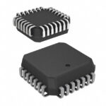 DG407BDN-T1
The activity of extra discounts on wholesale prices is in full swing…
Please fill in your contact information and we will send you the latest wholesale price list.





