 ChipApex | Global Electronic Components Supplier
DG413HSDY-T1
Search Product
Search Post
— IC芯片 | 连接器 | 传感器 | 被动器件 —
Search productSearch post
— IC芯片 | 连接器 | 传感器 | 被动器件 —
Consult the customer manager about the wholesale price.
consultation hotline:86-132-6715-2157
email:[email protected]
Contact the product manager for consultation. One-stop consultation is available.
Do you want a lower wholesale price? Please send us your inquiry and we will reply immediately.
The DG413HSDY-T1 is a precision monolithic quad SPST CMOS analog switch manufactured by Vishay Siliconix. It features four independent switches in a 16-pin narrow SOIC package, with two normally open and two normally closed channels. The device supports dual supplies up to ±20 V or single supplies up to 44 V. Key electrical parameters include a maximum on-resistance of 35 Ω at ±15 V, turn-on time of 105 ns, and turn-off time of 80 ns. It operates within a temperature range of -40 °C to +85 °C and consumes ultra-low power.
Verify the specific ordering suffix against official documentation to confirm package type and tape/reel specifications. Confirm RoHS compliance status for environmental requirements. Validate that the component meets the required operating temperature range for the intended application environment before finalizing procurement.
Select this component when high-speed switching and low distortion are critical for analog signal routing. Ensure the supply voltage does not exceed the 44 V absolute maximum rating. Consider the break-before-make timing characteristics if sequential channel switching is required to avoid signal overlap.
This part belongs to the DG411HS/DG412HS/DG413HS family of precision analog switches. The DG413 variant specifically combines two normally open and two normally closed switches, offering flexible signal routing configurations compared to the uniform polarity of the DG411 and DG412 models.
DG413HSDY-E3 (Tube packaging)
The break-before-make time delay is typically 20 ns at room temperature with a ±10 V supply.
Signals on S, D, or IN pins exceeding V+ or V- will be clamped by internal diodes. The forward diode current must be limited to the maximum current ratings.
The typical charge injection is 22 pC at room temperature with a 0 V ground reference and no source resistance.
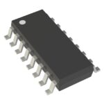 DG413HSDY-T1
The activity of extra discounts on wholesale prices is in full swing…
Please fill in your contact information and we will send you the latest wholesale price list.





