 ChipApex | Global Electronic Components Supplier

SEARCH
Search Product
Search Post
— IC芯片 | 连接器 | 传感器 | 被动器件 —
Search productSearch post
— IC芯片 | 连接器 | 传感器 | 被动器件 —
Consult the customer manager about the wholesale price.
consultation hotline:86-132-6715-2157
email:[email protected]
Contact the product manager for consultation. One-stop consultation is available.
Do you want a lower wholesale price? Please send us your inquiry and we will reply immediately.
HCF4035BEY is listed in the Shift Registers range at ChipApex. The manufacturer field lists STMicroelectronics. Its product description is IC SHIFT REG 4STG PAR I/O 16-DIP. Review the specifications below when checking this part for your BOM.
The HCF4035BEY is a monolithic integrated circuit fabricated in Metal Oxide Semiconductor technology, functioning as a four-stage parallel-in/parallel-out shift register. It features synchronous parallel entry on all stages and serial inputs to the first stage via JK logic. The device includes asynchronous true/complement control on all outputs and an asynchronous common reset. It operates with buffered inputs and outputs, supporting static flip-flop operation in a master-slave configuration. Recommended operating conditions specify a supply voltage range of 3V to 20V and an operating temperature range of -55°C to +125°C.
Verify that the ordering code matches HCF4035BEY for the DIP package variant. Confirm the datasheet version aligns with JEDEC JESD13B standards for B series CMOS devices. Ensure the application environment respects the absolute maximum ratings, particularly regarding power dissipation limits and voltage tolerances relative to VSS pin voltage.
Select this component when a four-stage shift register with both parallel and serial input capabilities is required. The inclusion of JK logic on the first stage makes it suitable for complex sequence generation without additional external gating. Consider the asynchronous true/complement control feature if simultaneous access to inverted data states is necessary within the system design.
This device belongs to the HCF4035B family of Monolithic Integrated Circuits. It is available in both DIP and SOP packages, with the BEY suffix indicating the specific DIP-16 physical form factor. The product line adheres to standardized specifications for B series CMOS devices, ensuring compatibility with other components in the same logical family.
HCF4035BM1 (SOP package)
The JK input logic on the first stage minimizes external logic requirements, particularly in counting and sequence generation applications. When connected together, the first stage functions as a D flip-flop.
When high, the true contents of the register are available at the output terminals. When low, the outputs provide the complements of the data in the register. This control functions asynchronously with respect to the clock signal.
Explore related parts through Logic, Integrated Circuits (ICs), all product categories, ChipApex homepage.
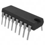 HCF4035BEY
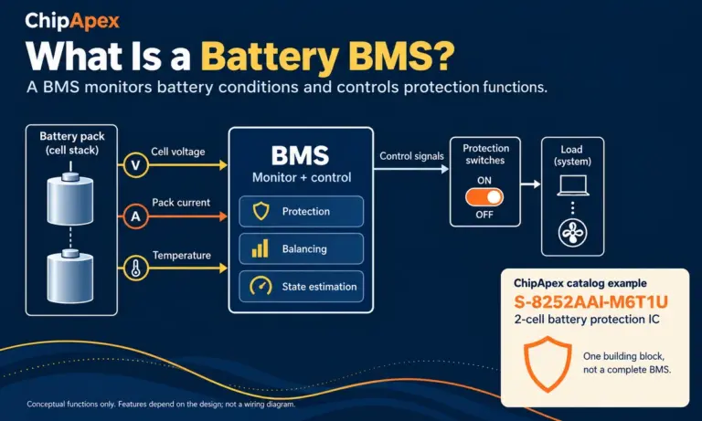
Learn what a battery BMS does, how protection differs from charging, and which pack specifications to check when sourcing BMS components through ChipApex.
Read More
HCF4035BEY is listed in the Shift Registers range at ChipApex. The manufacturer field lists STMicroelectronics. Its product description is IC SHIFT REG 4STG PAR…
Read More
HCF4035BEY is listed in the Shift Registers range at ChipApex. The manufacturer field lists STMicroelectronics. Its product description is IC SHIFT REG 4STG PAR…
Read More
HCF4035BEY is listed in the Shift Registers range at ChipApex. The manufacturer field lists STMicroelectronics. Its product description is IC SHIFT REG 4STG PAR…
Read More
HCF4035BEY is listed in the Shift Registers range at ChipApex. The manufacturer field lists STMicroelectronics. Its product description is IC SHIFT REG 4STG PAR…
Read More
Select a bridge rectifier by reverse voltage, capacitor charging current, startup surge and cooling. Work through a stated DC voltage and ripple example.
Read More
HCF4035BEY is listed in the Shift Registers range at ChipApex. The manufacturer field lists STMicroelectronics. Its product description is IC SHIFT REG 4STG PAR…
Read More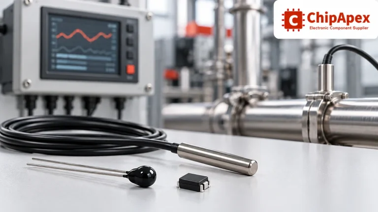
Compare thermistors, RTDs, thermocouples and temperature ICs. Learn how range, accuracy, response, interfaces and mounting affect component selection.
Read More
See how a MEMS gyroscope measures angular rate, why its angle estimate drifts, and which range, noise, interface and temperature specs to compare.
Read More
HCF4035BEY is listed in the Shift Registers range at ChipApex. The manufacturer field lists STMicroelectronics. Its product description is IC SHIFT REG 4STG PAR…
Read More
HCF4035BEY is listed in the Shift Registers range at ChipApex. The manufacturer field lists STMicroelectronics. Its product description is IC SHIFT REG 4STG PAR…
Read More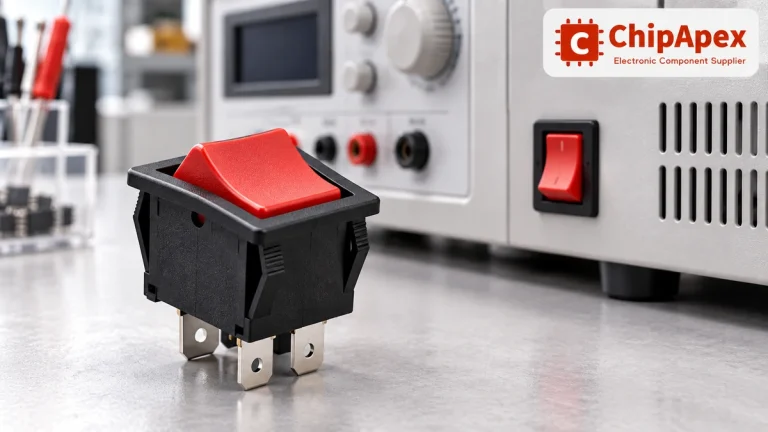
Choose a rocker switch by AC/DC ratings, contact arrangement, illumination, panel fit and sealing. Get practical checks for engineering and component sourcing.
Read More
The activity of extra discounts on wholesale prices is in full swing…
Please fill in your contact information and we will send you the latest wholesale price list.






