 ChipApex | Global Electronic Components Supplier

SEARCH
Search Product
Search Post
— IC芯片 | 连接器 | 传感器 | 被动器件 —
Search productSearch post
— IC芯片 | 连接器 | 传感器 | 被动器件 —
Consult the customer manager about the wholesale price.
consultation hotline:86-132-6715-2157
email:[email protected]
Contact the product manager for consultation. One-stop consultation is available.
Do you want a lower wholesale price? Please send us your inquiry and we will reply immediately.
HMC940LC4BTR is listed in the Clock Buffers, Drivers range at ChipApex. The manufacturer field lists Analog Devices Inc.. Its product description is IC CLOCK BUFFER 1:4 24SMT. Review the specifications below when checking this part for your BOM.
The HMC940LC4BTR is a high-speed 1:4 fanout buffer designed for data transmission rates up to 13 Gbps and clock frequencies as high as 13 GHz. It features differential CML inputs and outputs, with all signals DC coupled and internally terminated with 50-ohm resistors to ground. The device operates from a single -3.3V DC supply (range: -3.0V to -3.6V) and consumes approximately 133 mA of current. Key electrical parameters include a propagation delay of 101 ps, rise/fall times of 26/25 ps, and a programmable output voltage swing adjustable between 600 mV and 1400 mV via the VR pin.
Verify component authenticity through authorized Analog Devices channels or certified distributors. Confirm RoHS compliance status and REACH SVHC declarations prior to procurement. Ensure proper ESD handling precautions are observed during storage and assembly due to the device's sensitivity classification.
Select this component when designing circuits requiring a 1:4 signal distribution ratio at speeds exceeding 10 Gbps. Ensure the power supply provides a stable negative voltage within the -3.0V to -3.6V range. Verify that the PCB layout supports the 24-TFCQFN package dimensions and includes adequate thermal management for the exposed pad to handle 440 mW power dissipation.
This part belongs to the HMC940 series of high-speed digital logic components manufactured by Analog Devices Inc. It is specifically engineered for surface-mount technology (SMT) applications in ceramic packages. The TR suffix indicates it is supplied in Tape & Reel packaging format for automated assembly processes.
Publicly confirmed substitute part numbers are not available in the provided documentation. Evaluate alternative fanout buffers based on matching 13 Gbps speed capabilities, CML interface compatibility, and similar 24-lead QFN package footprints if direct replacement is required.
The output voltage level is controlled via the VR pin. Applying a specific voltage to this pin allows the user to adjust the differential output swing between 600 mV and 1400 mV.
Both the differential inputs and outputs are DC coupled and feature internal 50-ohm resistors connected to ground for termination.
The absolute maximum rating for the power supply voltage (Vee) is -3.75 V to +0.5 V.
Explore related parts through Clock/Timing, Integrated Circuits (ICs), all product categories, ChipApex homepage.
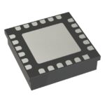 HMC940LC4BTR
Learn what an integrated circuit is, how ICs work, the main types and the specs to check before choosing a part for your design…
Read More
HMC940LC4BTR is listed in the Clock Buffers, Drivers range at ChipApex. The manufacturer field lists Analog Devices Inc.. Its product description is IC CLOCK…
Read More
HMC940LC4BTR is listed in the Clock Buffers, Drivers range at ChipApex. The manufacturer field lists Analog Devices Inc.. Its product description is IC CLOCK…
Read More
HMC940LC4BTR is listed in the Clock Buffers, Drivers range at ChipApex. The manufacturer field lists Analog Devices Inc.. Its product description is IC CLOCK…
Read More
Learn the relay definition, coil and contact operation, NO and NC forms, load ratings and suppression choices. Compare mechanical, reed and solid-state types.
Read More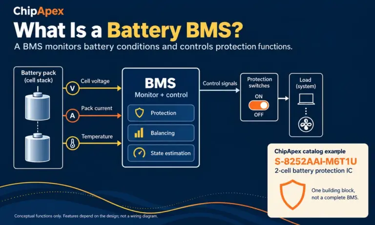
Learn what a battery BMS does, how protection differs from charging, and which pack specifications to check when sourcing BMS components through ChipApex.
Read More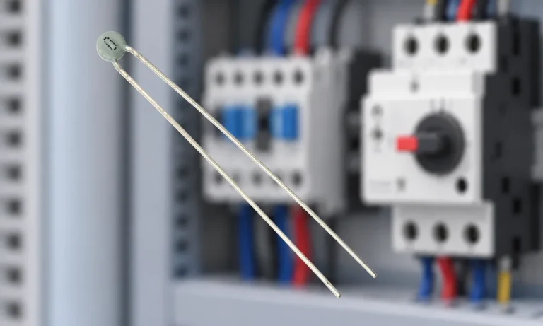
Learn why PTC resistance rises with temperature, how it differs from NTC, and which ratings matter for sensing and protection.
Read More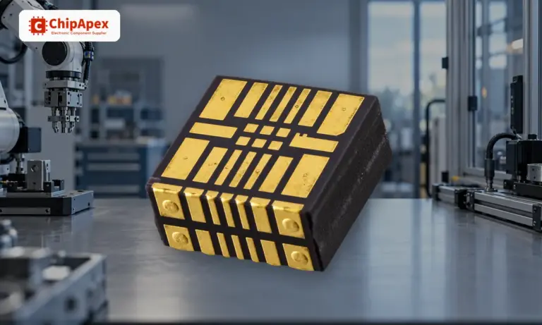
See how a MEMS gyroscope measures angular rate, why its angle estimate drifts, and which range, noise, interface and temperature specs to compare.
Read More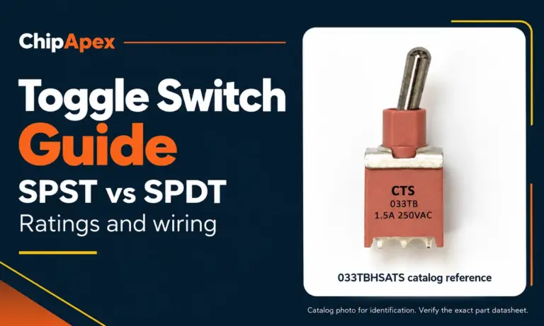
Compare SPST and SPDT toggle switches, understand AC/DC ratings, and follow wiring examples. Check contact action, mounting and parts in the ChipApex catalog.
Read More
HMC940LC4BTR is listed in the Clock Buffers, Drivers range at ChipApex. The manufacturer field lists Analog Devices Inc.. Its product description is IC CLOCK…
Read More
HMC940LC4BTR is listed in the Clock Buffers, Drivers range at ChipApex. The manufacturer field lists Analog Devices Inc.. Its product description is IC CLOCK…
Read More
HMC940LC4BTR is listed in the Clock Buffers, Drivers range at ChipApex. The manufacturer field lists Analog Devices Inc.. Its product description is IC CLOCK…
Read More
The activity of extra discounts on wholesale prices is in full swing…
Please fill in your contact information and we will send you the latest wholesale price list.




