 ChipApex | Global Electronic Components Supplier

SEARCH
Search Product
Search Post
— IC芯片 | 连接器 | 传感器 | 被动器件 —
Search productSearch post
— IC芯片 | 连接器 | 传感器 | 被动器件 —
Consult the customer manager about the wholesale price.
consultation hotline:86-132-6715-2157
email:[email protected]
Contact the product manager for consultation. One-stop consultation is available.
Do you want a lower wholesale price? Please send us your inquiry and we will reply immediately.
IPC020N10L3X1SA1 is listed in the Single FETs, MOSFETs range at ChipApex. The manufacturer field lists Infineon Technologies. Its product description is MOSFET N-CH 100V 1A SAWN ON FOIL. Review the specifications below when checking this part for your BOM.
The IPC020N10L3 is an N-channel enhancement mode OptiMOS™3 Power MOS Transistor Chip manufactured by Infineon Technologies. It features a die size of 2.1 x 0.96 mm² and a thickness of 220 µm. The device has a drain-source breakdown voltage (V(BR)DSS) of 100 V and a typical zero gate voltage drain current (IDSS) of 0.1 µA at VDS=100 V. The typical drain-source on-resistance (RDS(on)) is 42 mΩ at VGS=4.5 V and ID=2.0 A, with a maximum of 100 mΩ limited by wafer test equipment. Gate threshold voltage ranges from 1.1 V to 2.1 V. The reverse diode forward on-voltage is typically 1.0 V at IF=1 A. Single pulse avalanche energy (EAS) is rated at 184 mJ under specific conditions.
Verify the exact revision status of the datasheet before finalizing designs, as specifications may evolve. Confirm that the bare die format meets your assembly capabilities, including soldering or gluing requirements. Ensure electrostatic discharge precautions are strictly followed during handling, as the component is sensitive according to MIL-STD 883C standards. Validate thermal management strategies given the specific die dimensions and thickness provided in the documentation.
Select this component when a bare die solution is required rather than a packaged transistor. Consider the specific die dimensions of 2.1 x 0.96 mm² for footprint planning. Evaluate the RDS(on) characteristics at VGS=4.5 V against your circuit's drive voltage capabilities. Review the avalanche energy rating if transient robustness is a critical design parameter for the target application environment.
This part belongs to the OptiMOS™3 family of power MOS transistors designed for industrial and multimarket segments. Unlike packaged versions such as the BSZ440N10LS3 G, this component is supplied as a bare die. Designers must refer to related packaged products for dynamic characterization data, as the bare die itself does not include package parasitics. It serves as a foundational semiconductor element for custom power module integration.
No direct public substitute part numbers are listed in the source material. For packaged equivalents, reference documents point to the BSZ440N10LS3 G for dynamic characterization context, but it is a distinct packaged product. Custom die replacements require matching the 2.1 x 0.96 mm² die size and 100 V rating.
Explore related parts through FETs, MOSFETs, Transistors, Discrete Semiconductor Products, all product categories.
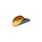 IPC020N10L3X1SA1

Choose an AC to DC converter by input range, output demand, isolation, efficiency and thermal derating. Compare architectures and check installation needs.
Read More
IPC020N10L3X1SA1 is listed in the Single FETs, MOSFETs range at ChipApex. The manufacturer field lists Infineon Technologies. Its product description is MOSFET N-CH 100V…
Read More
See how a MEMS gyroscope measures angular rate, why its angle estimate drifts, and which range, noise, interface and temperature specs to compare.
Read More
IPC020N10L3X1SA1 is listed in the Single FETs, MOSFETs range at ChipApex. The manufacturer field lists Infineon Technologies. Its product description is MOSFET N-CH 100V…
Read More
IPC020N10L3X1SA1 is listed in the Single FETs, MOSFETs range at ChipApex. The manufacturer field lists Infineon Technologies. Its product description is MOSFET N-CH 100V…
Read More
IPC020N10L3X1SA1 is listed in the Single FETs, MOSFETs range at ChipApex. The manufacturer field lists Infineon Technologies. Its product description is MOSFET N-CH 100V…
Read More
IPC020N10L3X1SA1 is listed in the Single FETs, MOSFETs range at ChipApex. The manufacturer field lists Infineon Technologies. Its product description is MOSFET N-CH 100V…
Read More
IPC020N10L3X1SA1 is listed in the Single FETs, MOSFETs range at ChipApex. The manufacturer field lists Infineon Technologies. Its product description is MOSFET N-CH 100V…
Read More
IPC020N10L3X1SA1 is listed in the Single FETs, MOSFETs range at ChipApex. The manufacturer field lists Infineon Technologies. Its product description is MOSFET N-CH 100V…
Read More
IPC020N10L3X1SA1 is listed in the Single FETs, MOSFETs range at ChipApex. The manufacturer field lists Infineon Technologies. Its product description is MOSFET N-CH 100V…
Read More
IPC020N10L3X1SA1 is listed in the Single FETs, MOSFETs range at ChipApex. The manufacturer field lists Infineon Technologies. Its product description is MOSFET N-CH 100V…
Read More
IPC020N10L3X1SA1 is listed in the Single FETs, MOSFETs range at ChipApex. The manufacturer field lists Infineon Technologies. Its product description is MOSFET N-CH 100V…
Read More
The activity of extra discounts on wholesale prices is in full swing…
Please fill in your contact information and we will send you the latest wholesale price list.





