ChipApex | Global Electronic Components Supplier

SEARCH
Search Product
Search Post
— IC芯片 | 连接器 | 传感器 | 被动器件 —
Search productSearch post
— IC芯片 | 连接器 | 传感器 | 被动器件 —
Consult the customer manager about the wholesale price.
consultation hotline:86-132-6715-2157
email:[email protected]
Contact the product manager for consultation. One-stop consultation is available.
Do you want a lower wholesale price? Please send us your inquiry and we will reply immediately.
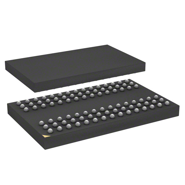
IS42S32400B-6BL is listed in the Memory IC range at ChipApex. The manufacturer field lists ISSI, Integrated Silicon Solution Inc. Its product description is IC DRAM 128MBIT PAR 90TFBGA. Review the specifications below when checking this part for your BOM.
The IS42S32400B is a 128Mb Synchronous DRAM organized as 4 Meg x 32 bits across four internal banks. It supports clock frequencies of 166, 143, 125, and 100 MHz with CAS latencies of 2 or 3 clocks. The device operates on 3.3V VDD and VDDQ supplies within a -40°C to +85°C industrial temperature range. Access times are 5.4 ns for CL=3 and 6.5 ns for CL=2. Available in 86-pin TSOP-II and 90-ball FBGA packages.
Verify the specific speed grade suffix (-6 or -7) required for your target clock frequency. Confirm package selection between TSOP-II and FBGA based on board layout constraints. Check current lifecycle status as this component may be subject to discontinuation. Ensure voltage levels match the 3.3V specification strictly.
Select the -6 variant for 166 MHz operation or -7 for 143 MHz. Choose the FBGA package for surface mount density or TSOP-II for alternative form factors. Verify that the system design accommodates the 3.3V I/O requirements and LVTTL compatibility. Consider thermal dissipation capabilities for the chosen package type under maximum load conditions.
This component belongs to ISSI's 128Mb SDRAM family, designed for high-performance synchronous memory applications. It utilizes a CMOS process technology optimized for low power consumption while maintaining high data throughput rates suitable for complex digital signal processing and computing environments.
Check for IS42S32400D or IS42S32400J variants which share similar specifications but may differ in package availability or exact timing parameters. Ensure any substitute maintains the 32-bit width and 128Mb capacity.
Auto Precharge initiates at the end of a READ or WRITE burst when A10 is HIGH, automatically closing the accessed row without requiring an explicit PRECHARGE command.
DQM0-DQM3 control the four bytes of the I/O buffers, enabling or disabling data output during reads and masking input data during writes.
Explore related parts through Memory, Integrated Circuits (ICs), all product categories, ChipApex homepage.
 IS42S32400B-6BL

Choose an AC to DC converter by input range, output demand, isolation, efficiency and thermal derating. Compare architectures and check installation needs.
Read More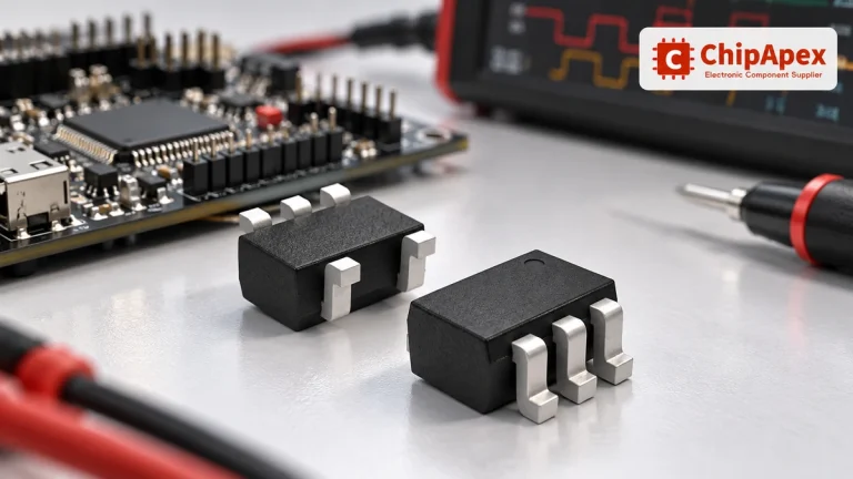
Choose logic inverter ICs by thresholds, supply, output drive and delay. Compare standard and Schmitt-trigger inputs, power sequencing and replacement checks.
Read More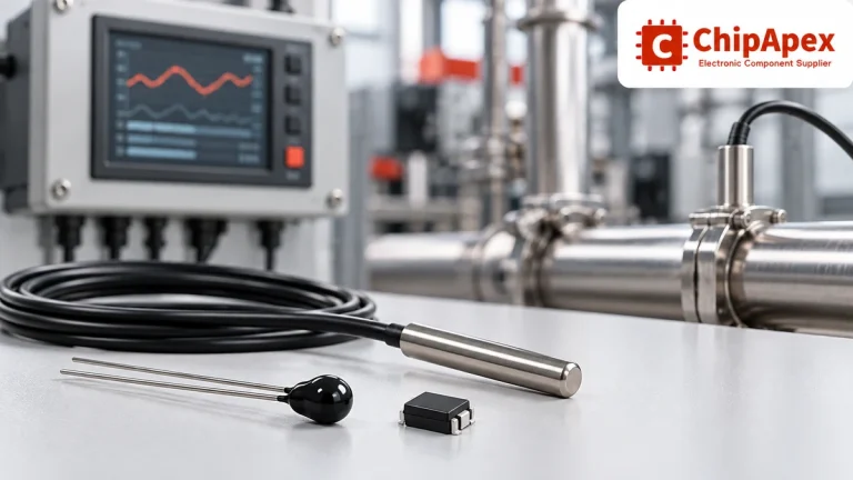
Compare thermistors, RTDs, thermocouples and temperature ICs. Learn how range, accuracy, response, interfaces and mounting affect component selection.
Read More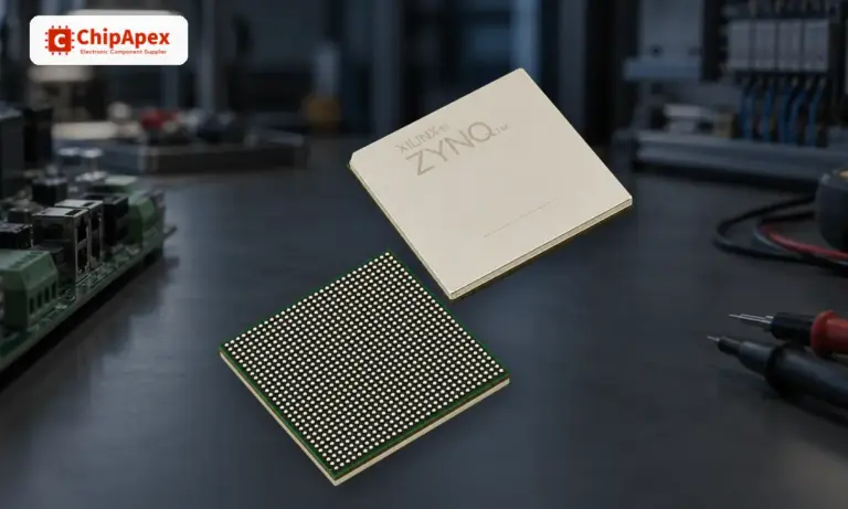
Learn what an integrated circuit is, how ICs work, the main types and the specs to check before choosing a part for your design…
Read More
IS42S32400B-6BL is listed in the Memory IC range at ChipApex. The manufacturer field lists ISSI, Integrated Silicon Solution Inc. Its product description is IC…
Read More
IS42S32400B-6BL is listed in the Memory IC range at ChipApex. The manufacturer field lists ISSI, Integrated Silicon Solution Inc. Its product description is IC…
Read More
IS42S32400B-6BL is listed in the Memory IC range at ChipApex. The manufacturer field lists ISSI, Integrated Silicon Solution Inc. Its product description is IC…
Read More
See how a MEMS gyroscope measures angular rate, why its angle estimate drifts, and which range, noise, interface and temperature specs to compare.
Read More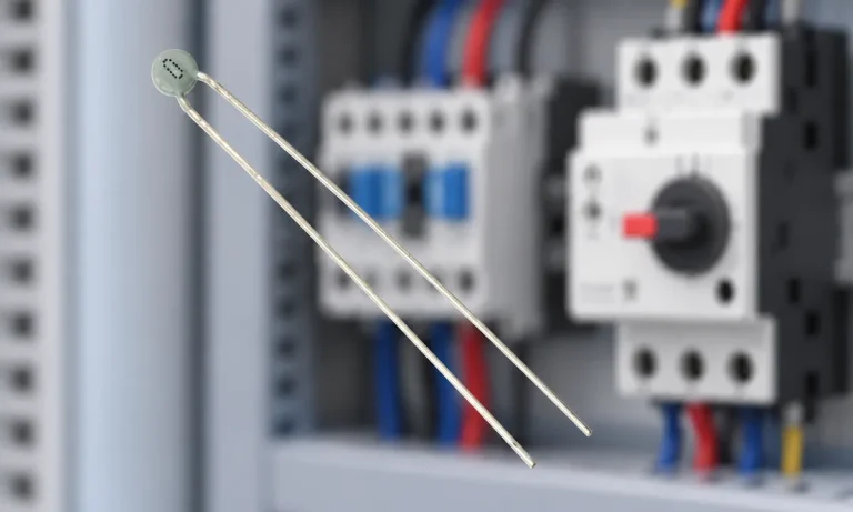
Learn why PTC resistance rises with temperature, how it differs from NTC, and which ratings matter for sensing and protection.
Read More
IS42S32400B-6BL is listed in the Memory IC range at ChipApex. The manufacturer field lists ISSI, Integrated Silicon Solution Inc. Its product description is IC…
Read More
IS42S32400B-6BL is listed in the Memory IC range at ChipApex. The manufacturer field lists ISSI, Integrated Silicon Solution Inc. Its product description is IC…
Read More
IS42S32400B-6BL is listed in the Memory IC range at ChipApex. The manufacturer field lists ISSI, Integrated Silicon Solution Inc. Its product description is IC…
Read More
The activity of extra discounts on wholesale prices is in full swing…
Please fill in your contact information and we will send you the latest wholesale price list.