ChipApex | Global Electronic Components Supplier

SEARCH
Search Product
Search Post
— IC芯片 | 连接器 | 传感器 | 被动器件 —
Search productSearch post
— IC芯片 | 连接器 | 传感器 | 被动器件 —
Consult the customer manager about the wholesale price.
consultation hotline:86-132-6715-2157
email:[email protected]
Contact the product manager for consultation. One-stop consultation is available.
Do you want a lower wholesale price? Please send us your inquiry and we will reply immediately.
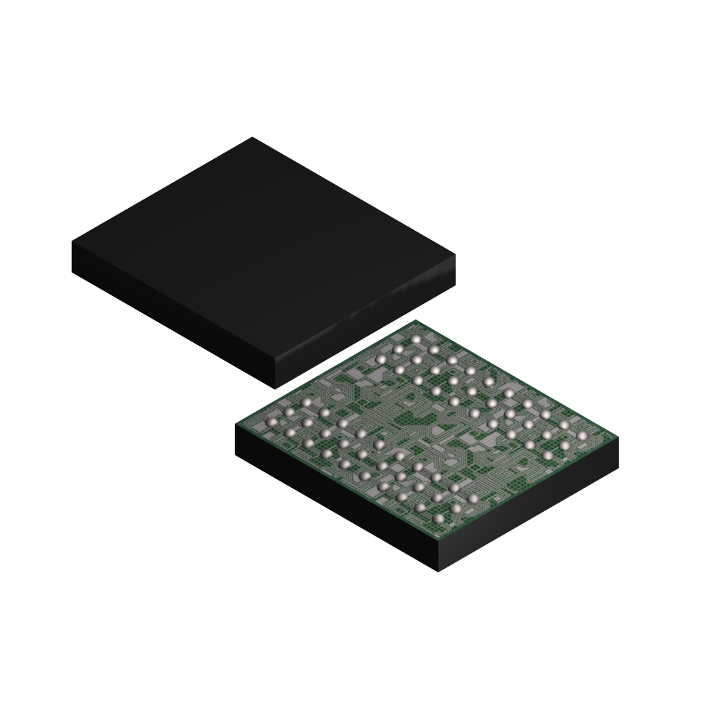
JSD12164PAH-50-SU is listed in the Memory IC range at ChipApex. The manufacturer field lists Jeju Semiconductor Corp. Its product description is 512M LPDDR1 PKG 8x9mm 60B BGA. Review the specifications below when checking this part for your BOM.
The JSD12164PAH-50-SU is a 512Mb LPDDR SDRAM manufactured by Jeju Semiconductor Corp. It features a synchronous double data rate architecture with a 2n-prefetch interface, transferring two data words per clock cycle at the I/O balls. The device operates within a voltage range of 1.7V to 1.95V for both VDD and VDDQ. It supports x16 and x32 data widths with clock rates up to 200MHz. Internal organization consists of four banks, each containing 134,217,728 bits arranged as 8,192 rows by 1,024 columns by 16 bits or 8,192 rows by 512 columns by 32 bits.
Verify that the specific ordering suffix matches the required package type and temperature grade. Confirm compatibility with system power sequencing requirements, specifically simultaneous VDD and VDDQ ramp-up. Ensure initialization sequences adhere to the specified timing parameters to prevent undefined operation.
Select this component based on the required data width (x16 or x32) and operating frequency constraints. Consider the available package options, such as the 60-ball FPBGA for x16 configurations. Evaluate the need for PASR and ATCSR features if power efficiency in self-refresh modes is critical for the target application.
This part belongs to the JSD12XX4PAx-SU family of 512Mb LPDDR SDRAMs. The series utilizes high-performance CMOS technology and is designed for mobile and embedded applications. Variants within the family differ primarily in data width and physical package dimensions while maintaining the core double data rate architecture.
No public confirmed substitute part numbers are documented in the provided source material.
PASR is configured via the Extended Mode Register using address bits A0 to A2. Options include refreshing the entire array, 1/2 array, 1/4 array, or smaller fractions, with data outside the defined area being lost.
The device core power (VDD) and I/O power (VDDQ) must be brought up simultaneously to prevent latch-up. It is recommended that both voltages originate from the same power source.
Explore related parts through Memory, Integrated Circuits (ICs), all product categories, ChipApex homepage.
 JSD12164PAH-50-SU
Find out when a bare shock switch needs a pull resistor, when an MCU internal pull-up is enough, and why sensor modules and piezo…
Read More
JSD12164PAH-50-SU is listed in the Memory IC range at ChipApex. The manufacturer field lists Jeju Semiconductor Corp. Its product description is 512M LPDDR1 PKG…
Read More
JSD12164PAH-50-SU is listed in the Memory IC range at ChipApex. The manufacturer field lists Jeju Semiconductor Corp. Its product description is 512M LPDDR1 PKG…
Read More
JSD12164PAH-50-SU is listed in the Memory IC range at ChipApex. The manufacturer field lists Jeju Semiconductor Corp. Its product description is 512M LPDDR1 PKG…
Read More
JSD12164PAH-50-SU is listed in the Memory IC range at ChipApex. The manufacturer field lists Jeju Semiconductor Corp. Its product description is 512M LPDDR1 PKG…
Read More
JSD12164PAH-50-SU is listed in the Memory IC range at ChipApex. The manufacturer field lists Jeju Semiconductor Corp. Its product description is 512M LPDDR1 PKG…
Read More
JSD12164PAH-50-SU is listed in the Memory IC range at ChipApex. The manufacturer field lists Jeju Semiconductor Corp. Its product description is 512M LPDDR1 PKG…
Read More
JSD12164PAH-50-SU is listed in the Memory IC range at ChipApex. The manufacturer field lists Jeju Semiconductor Corp. Its product description is 512M LPDDR1 PKG…
Read More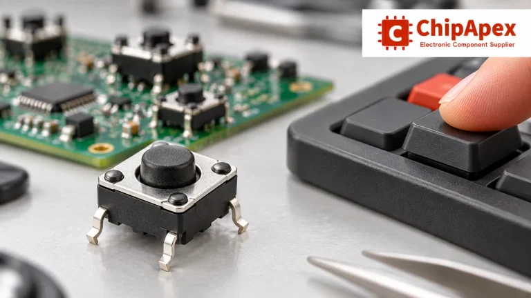
Understand tactile switches, PCB and keyboard differences, four-pin wiring, debounce, force, travel and replacement checks for reliable control inputs.
Read More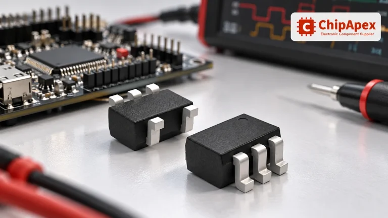
Choose logic inverter ICs by thresholds, supply, output drive and delay. Compare standard and Schmitt-trigger inputs, power sequencing and replacement checks.
Read More
Choose an AC to DC converter by input range, output demand, isolation, efficiency and thermal derating. Compare architectures and check installation needs.
Read More
Understand RF attenuator dB values, fixed and programmable types, impedance, power limits and noise tradeoffs before choosing parts for an RF signal path.
Read More
The activity of extra discounts on wholesale prices is in full swing…
Please fill in your contact information and we will send you the latest wholesale price list.