 ChipApex | Global Electronic Components Supplier

SEARCH
Search Product
Search Post
— IC芯片 | 连接器 | 传感器 | 被动器件 —
Search productSearch post
— IC芯片 | 连接器 | 传感器 | 被动器件 —
Consult the customer manager about the wholesale price.
consultation hotline:86-132-6715-2157
email:[email protected]
Contact the product manager for consultation. One-stop consultation is available.
Do you want a lower wholesale price? Please send us your inquiry and we will reply immediately.
LFEC33E-5FN484C is listed in the Field Programmable Gate Array range at ChipApex. The manufacturer field lists Lattice Semiconductor Corporation. Its product description is IC FPGA 360 I/O 484FBGA. Review the specifications below when checking this part for your BOM.
The LFE3-35EA-6FN484C is a Field Programmable Gate Array from the LatticeLFE3 series, manufactured by Lattice Semiconductor Corporation. It features 33,000 logic elements and 16,500 Adaptive Logic Modules (ALMs). The device includes 1.3 Mbits of embedded memory, comprising 1,327 kbits of Embedded Block RAM (EBR) and 68 kbits of distributed RAM. It supports up to 295 I/Os and operates at a maximum frequency of 375 MHz with data rates up to 3.2 Gb/s. The core voltage is 1.2 V, ranging from 1.14 V to 1.26 V. Operating temperatures range from 0°C to +85°C. It is housed in an FPBGA-484 package.
Verify component authenticity through authorized distributors or direct manufacturer channels. Confirm RoHS compliance status and moisture sensitivity levels prior to assembly. Ensure storage conditions meet humidity requirements to prevent damage during PCB placement processes.
Select this model when designs require moderate logic density combined with high-speed serial connectivity. Compare against LFE2 series for legacy compatibility or ECP3 series for higher performance needs. Verify pinout compatibility if migrating from previous FPGA generations within the same package footprint.
This component belongs to the LatticeLFE3 family, designed for cost-effective mainstream applications. It bridges the gap between lower-density LFE2 devices and higher-performance ECP3 families. The -6 speed grade indicates specific timing characteristics suitable for general-purpose logic and interface bridging tasks.
Direct substitutes include other LFE3-35EA variants with different speed grades or package options. Cross-family migration may require schematic adjustments due to differing pinouts between LFE2 and LFE3 series.
Explore related parts through Embedded, Integrated Circuits (ICs), all product categories, ChipApex homepage.


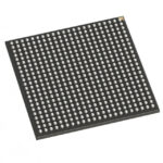 LFEC33E-5FN484C

See how a MEMS gyroscope measures angular rate, why its angle estimate drifts, and which range, noise, interface and temperature specs to compare.
Read More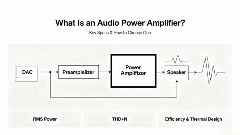
LFEC33E-5FN484C is listed in the Field Programmable Gate Array range at ChipApex. The manufacturer field lists Lattice Semiconductor Corporation. Its product description is IC…
Read More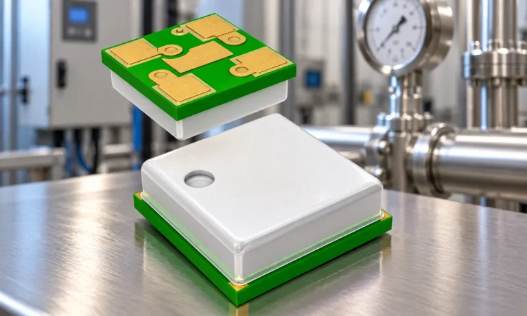
Learn how a pressure transducer converts pressure into voltage, current, or digital output, and compare pressure references and key selection specs.
Read More
Compare RC, crystal and MEMS oscillator circuits. Check ppm, jitter, load capacitance, startup margin and output compatibility before choosing a clock source.
Read More
LFEC33E-5FN484C is listed in the Field Programmable Gate Array range at ChipApex. The manufacturer field lists Lattice Semiconductor Corporation. Its product description is IC…
Read More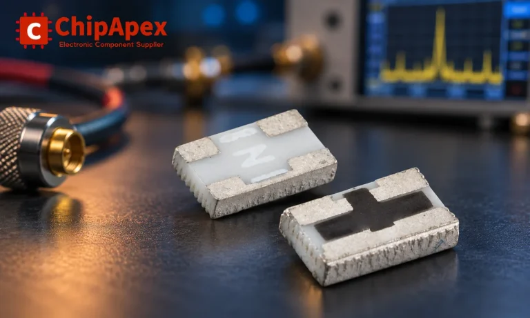
Understand RF attenuator dB values, fixed and programmable types, impedance, power limits and noise tradeoffs before choosing parts for an RF signal path.
Read More
LFEC33E-5FN484C is listed in the Field Programmable Gate Array range at ChipApex. The manufacturer field lists Lattice Semiconductor Corporation. Its product description is IC…
Read More
LFEC33E-5FN484C is listed in the Field Programmable Gate Array range at ChipApex. The manufacturer field lists Lattice Semiconductor Corporation. Its product description is IC…
Read More
LFEC33E-5FN484C is listed in the Field Programmable Gate Array range at ChipApex. The manufacturer field lists Lattice Semiconductor Corporation. Its product description is IC…
Read More
LFEC33E-5FN484C is listed in the Field Programmable Gate Array range at ChipApex. The manufacturer field lists Lattice Semiconductor Corporation. Its product description is IC…
Read More
LFEC33E-5FN484C is listed in the Field Programmable Gate Array range at ChipApex. The manufacturer field lists Lattice Semiconductor Corporation. Its product description is IC…
Read More
LFEC33E-5FN484C is listed in the Field Programmable Gate Array range at ChipApex. The manufacturer field lists Lattice Semiconductor Corporation. Its product description is IC…
Read More
The activity of extra discounts on wholesale prices is in full swing…
Please fill in your contact information and we will send you the latest wholesale price list.



