ChipApex | Global Electronic Components Supplier

SEARCH
Search Product
Search Post
— IC芯片 | 连接器 | 传感器 | 被动器件 —
Search productSearch post
— IC芯片 | 连接器 | 传感器 | 被动器件 —
Consult the customer manager about the wholesale price.
consultation hotline:86-132-6715-2157
email:[email protected]
Contact the product manager for consultation. One-stop consultation is available.
Do you want a lower wholesale price? Please send us your inquiry and we will reply immediately.
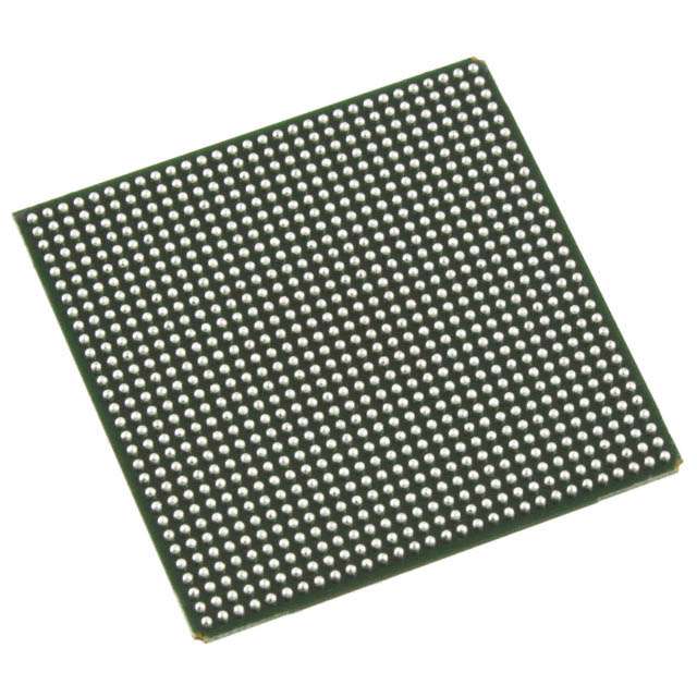
LFSCM3GA25EP1-6FN900C is listed in the Field Programmable Gate Array range at ChipApex. The manufacturer field lists Lattice Semiconductor Corporation. Its product description is IC FPGA 378 I/O 900FBGA. Review the specifications below when checking this part for your BOM.
The LFSCM3GA25EP1-6FN900C is a Field Programmable Gate Array (FPGA) belonging to the LatticeSC/M family. It features embedded high-speed SERDES and large embedded RAM within a single industry-standard package. The device supports high-performance I/Os and includes advanced clock management resources, designed for demanding communication network applications.
Verify component status as this specific part number may be obsolete or end-of-life. Confirm availability through authorized distributors only. Check for halogen-free substrate compliance if required by project specifications. Ensure compatibility with existing design tools and programming hardware before procurement.
Select this component for designs requiring integrated SERDES capabilities alongside substantial logic resources. Consider the LatticeSC/M family benefits for low-power requirements compared to other FPGA families. Evaluate pin count and I/O density against system interface needs. Verify thermal performance within the target operating temperature range.
This device is part of the LatticeSC/M series, which targets high-end system designs. The family combines FPGA fabric with ASIC-like performance blocks. It is positioned for applications needing high throughput and low latency in networking and industrial sectors.
Check for direct substitutes within the LatticeSC/M family such as LFSCM3GA25E variants. Review PCN documents for any package or material changes. Consult official Lattice documentation for recommended obsolescence alternatives.
Explore related parts through Embedded, Integrated Circuits (ICs), all product categories, ChipApex homepage.
 LFSCM3GA25EP1-6FN900C

LFSCM3GA25EP1-6FN900C is listed in the Field Programmable Gate Array range at ChipApex. The manufacturer field lists Lattice Semiconductor Corporation. Its product description is IC…
Read More
LFSCM3GA25EP1-6FN900C is listed in the Field Programmable Gate Array range at ChipApex. The manufacturer field lists Lattice Semiconductor Corporation. Its product description is IC…
Read More
LFSCM3GA25EP1-6FN900C is listed in the Field Programmable Gate Array range at ChipApex. The manufacturer field lists Lattice Semiconductor Corporation. Its product description is IC…
Read More
LFSCM3GA25EP1-6FN900C is listed in the Field Programmable Gate Array range at ChipApex. The manufacturer field lists Lattice Semiconductor Corporation. Its product description is IC…
Read More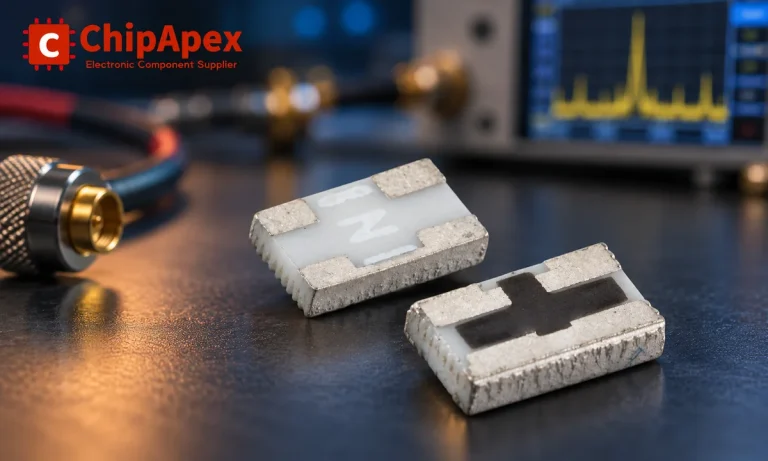
Understand RF attenuator dB values, fixed and programmable types, impedance, power limits and noise tradeoffs before choosing parts for an RF signal path.
Read More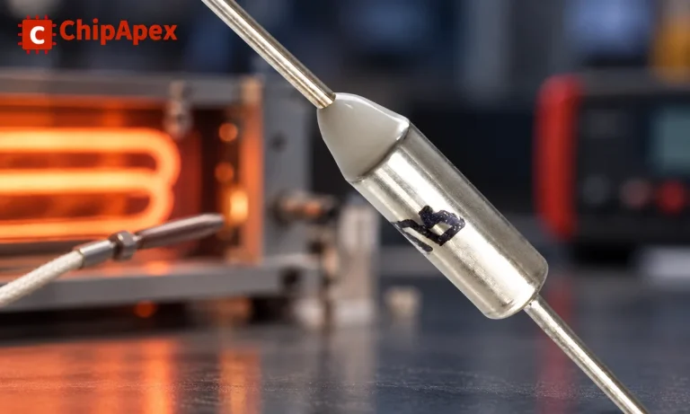
Understand thermal fuse operation, Tf, Th and Tm, electrical ratings and mounting. Check temperature limits and replacement requirements for your design.
Read More
LFSCM3GA25EP1-6FN900C is listed in the Field Programmable Gate Array range at ChipApex. The manufacturer field lists Lattice Semiconductor Corporation. Its product description is IC…
Read More
LFSCM3GA25EP1-6FN900C is listed in the Field Programmable Gate Array range at ChipApex. The manufacturer field lists Lattice Semiconductor Corporation. Its product description is IC…
Read More
LFSCM3GA25EP1-6FN900C is listed in the Field Programmable Gate Array range at ChipApex. The manufacturer field lists Lattice Semiconductor Corporation. Its product description is IC…
Read More
LFSCM3GA25EP1-6FN900C is listed in the Field Programmable Gate Array range at ChipApex. The manufacturer field lists Lattice Semiconductor Corporation. Its product description is IC…
Read More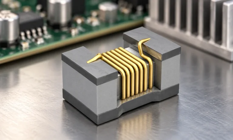
See when an inductor behaves linearly, how DC bias and saturation reduce inductance, and which current and temperature curves to check.
Read More
Learn what an IMU measures, how accelerometers and gyroscopes work together, why orientation estimates drift, and what to compare.
Read More
The activity of extra discounts on wholesale prices is in full swing…
Please fill in your contact information and we will send you the latest wholesale price list.