 ChipApex | Global Electronic Components Supplier

SEARCH
Search Product
Search Post
— IC芯片 | 连接器 | 传感器 | 被动器件 —
Search productSearch post
— IC芯片 | 连接器 | 传感器 | 被动器件 —
Consult the customer manager about the wholesale price.
consultation hotline:86-132-6715-2157
email:[email protected]
Contact the product manager for consultation. One-stop consultation is available.
Do you want a lower wholesale price? Please send us your inquiry and we will reply immediately.
LFXP20C-3FN484I is listed in the Field Programmable Gate Array range at ChipApex. The manufacturer field lists Lattice Semiconductor Corporation. Its product description is IC FPGA 340 I/O 484FBGA. Review the specifications below when checking this part for your BOM.
The LFXP20C-3FN484I is a Field Programmable Gate Array from the LatticeXP family, manufactured by Lattice Semiconductor Corporation. It features 19.7K logic elements and supports up to 340 I/Os in a 484-ball fpBGA package. The device operates with VCC voltages of 1.2V, 1.8V, 2.5V, or 3.3V. It includes 396 Kbits of sysMEM Embedded Block RAM and 79 Kbits of distributed RAM. The architecture provides four sysCLOCK PLLs for clock management.
Verify the specific ordering suffix against official documentation to confirm package type and temperature range. Ensure compatibility with existing board layouts for the 484-ball fpBGA form factor. Confirm that the selected voltage supply aligns with the device's support for 1.2V, 1.8V, 2.5V, or 3.3V operations as defined in the datasheet.
Select this component when a balance of moderate logic density and extensive I/O count is required. The LFXP20 offers 19.7K LUTs suitable for complex control logic. Consider the family's non-volatile nature if instant-on functionality is critical. Verify that the 340 I/O limit meets interface requirements before choosing over higher-density variants.
This part belongs to the LatticeXP family, which utilizes ispXP technology for non-volatile, infinitely reconfigurable logic. The family ranges from 3.1K to 19.7K LUTs, offering density migration options. The LFXP20 represents the highest density within this specific series, providing significant resources for embedded memory and processing tasks.
LFXP20E-4FN484I
Explore related parts through Embedded, Integrated Circuits (ICs), all product categories, ChipApex homepage.
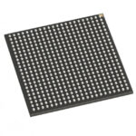 LFXP20C-3FN484I
Understand tactile switches, PCB and keyboard differences, four-pin wiring, debounce, force, travel and replacement checks for reliable control inputs.
Read More
Compare RC, crystal and MEMS oscillator circuits. Check ppm, jitter, load capacitance, startup margin and output compatibility before choosing a clock source.
Read More
LFXP20C-3FN484I is listed in the Field Programmable Gate Array range at ChipApex. The manufacturer field lists Lattice Semiconductor Corporation. Its product description is IC…
Read More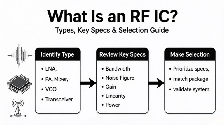
LFXP20C-3FN484I is listed in the Field Programmable Gate Array range at ChipApex. The manufacturer field lists Lattice Semiconductor Corporation. Its product description is IC…
Read More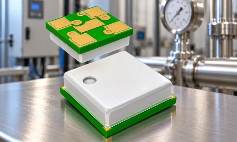
Learn how a pressure transducer converts pressure into voltage, current, or digital output, and compare pressure references and key selection specs.
Read More
LFXP20C-3FN484I is listed in the Field Programmable Gate Array range at ChipApex. The manufacturer field lists Lattice Semiconductor Corporation. Its product description is IC…
Read More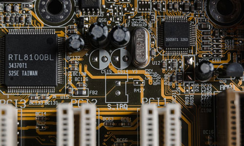
LFXP20C-3FN484I is listed in the Field Programmable Gate Array range at ChipApex. The manufacturer field lists Lattice Semiconductor Corporation. Its product description is IC…
Read More
LFXP20C-3FN484I is listed in the Field Programmable Gate Array range at ChipApex. The manufacturer field lists Lattice Semiconductor Corporation. Its product description is IC…
Read More
LFXP20C-3FN484I is listed in the Field Programmable Gate Array range at ChipApex. The manufacturer field lists Lattice Semiconductor Corporation. Its product description is IC…
Read More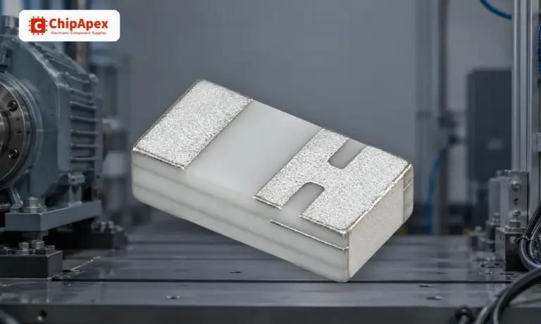
Find out when a bare shock switch needs a pull resistor, when an MCU internal pull-up is enough, and why sensor modules and piezo…
Read More
Choose logic inverter ICs by thresholds, supply, output drive and delay. Compare standard and Schmitt-trigger inputs, power sequencing and replacement checks.
Read More
LFXP20C-3FN484I is listed in the Field Programmable Gate Array range at ChipApex. The manufacturer field lists Lattice Semiconductor Corporation. Its product description is IC…
Read More
The activity of extra discounts on wholesale prices is in full swing…
Please fill in your contact information and we will send you the latest wholesale price list.






