 ChipApex | Global Electronic Components Supplier

SEARCH
Search Product
Search Post
— IC芯片 | 连接器 | 传感器 | 被动器件 —
Search productSearch post
— IC芯片 | 连接器 | 传感器 | 被动器件 —
Consult the customer manager about the wholesale price.
consultation hotline:86-132-6715-2157
email:[email protected]
Contact the product manager for consultation. One-stop consultation is available.
Do you want a lower wholesale price? Please send us your inquiry and we will reply immediately.
LMK1D1208IRHAR is listed in the Clock Buffers, Drivers range at ChipApex. The manufacturer field lists Texas Instruments. Its product description is IC CLK BUFFER 2:8 2GHZ 40VQFN. Review the specifications below when checking this part for your BOM.
The LMK1D1208IRHAR is an I2C-configurable, low-additive jitter LVDS clock buffer manufactured by Texas Instruments. It features two selectable inputs and eight differential LVDS output pairs (OUT0–OUT7) housed in a 6-mm × 6-mm, 40-pin VQFN package. The device supports supply voltages of 1.8 V, 2.5 V, or 3.3 V ± 5% and operates within an industrial temperature range of –40°C to +105°C. Key electrical specifications include a maximum output frequency of 2 GHz, additive jitter of less than 60 fs RMS (measured at 156.25 MHz with a 12 kHz to 20 MHz integration bandwidth), and a typical phase noise floor of -164 dBc/Hz. Propagation delay is maintained below 575 ps, with output skew limited to 20 ps maximum.
Verify the ordering suffix 'RHAR' corresponds to the specific 40-pin VQFN package variant required for the design. Confirm that the I2C address configuration via IDX0 and IDX1 pins aligns with the system's bus topology. Ensure power supply decoupling meets the recommended operating conditions for the selected voltage rail (1.8 V, 2.5 V, or 3.3 V). Check thermal management requirements given the junction-to-ambient thermal resistance of 39.1 °C/W.
Select the LMK1D1208IRHAR over pin-controlled variants (such as LMK1D1208P) when dynamic reconfiguration of output banks, individual channel enabling, or variable output swing is required during operation. This model is suitable for applications needing precise duty cycle control and low additive jitter (<60 fs RMS) compared to standard buffers. Consider the 40-pin package size if board space allows, as it offers more flexibility than the 28-pin LMK1D1208.
The LMK1D1208I belongs to the LMK1D12xx family of low-additive jitter LVDS buffers. Unlike the standard LMK1D1208 which uses pin-controlled global output enable, this I-suffix variant provides granular control via I2C registers. It shares the same core performance metrics, such as the 2 GHz output frequency and <575 ps propagation delay, but distinguishes itself through software-defined configurability for complex clock distribution networks.
LMK1D1208PRHAR: Pin-compatible alternative with identical package but controlled via hardware pins rather than I2C. LMK1D1208RHDT: Standard version with 28-pin VQFN package; requires schematic and layout redesign due to different pinout and package dimensions.
Explore related parts through Clock/Timing, Integrated Circuits (ICs), all product categories, ChipApex homepage.
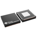 LMK1D1208IRHAR
LMK1D1208IRHAR is listed in the Clock Buffers, Drivers range at ChipApex. The manufacturer field lists Texas Instruments. Its product description is IC CLK BUFFER…
Read More
LMK1D1208IRHAR is listed in the Clock Buffers, Drivers range at ChipApex. The manufacturer field lists Texas Instruments. Its product description is IC CLK BUFFER…
Read More
LMK1D1208IRHAR is listed in the Clock Buffers, Drivers range at ChipApex. The manufacturer field lists Texas Instruments. Its product description is IC CLK BUFFER…
Read More
LMK1D1208IRHAR is listed in the Clock Buffers, Drivers range at ChipApex. The manufacturer field lists Texas Instruments. Its product description is IC CLK BUFFER…
Read More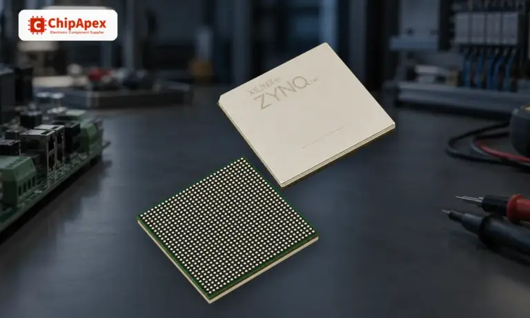
Learn what an integrated circuit is, how ICs work, the main types and the specs to check before choosing a part for your design…
Read More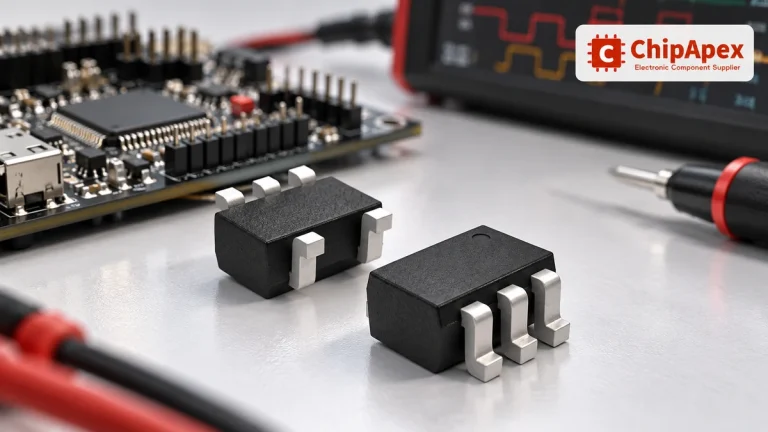
Choose logic inverter ICs by thresholds, supply, output drive and delay. Compare standard and Schmitt-trigger inputs, power sequencing and replacement checks.
Read More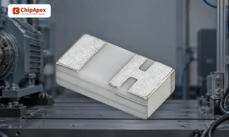
Find out when a bare shock switch needs a pull resistor, when an MCU internal pull-up is enough, and why sensor modules and piezo…
Read More
LMK1D1208IRHAR is listed in the Clock Buffers, Drivers range at ChipApex. The manufacturer field lists Texas Instruments. Its product description is IC CLK BUFFER…
Read More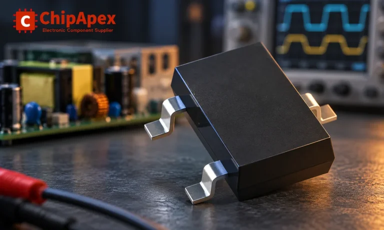
Learn how rectifiers convert AC to DC, compare half-wave and bridge circuits, and select voltage, current, recovery and thermal ratings for your design.
Read More
Select a bridge rectifier by reverse voltage, capacitor charging current, startup surge and cooling. Work through a stated DC voltage and ripple example.
Read More
LMK1D1208IRHAR is listed in the Clock Buffers, Drivers range at ChipApex. The manufacturer field lists Texas Instruments. Its product description is IC CLK BUFFER…
Read More
LMK1D1208IRHAR is listed in the Clock Buffers, Drivers range at ChipApex. The manufacturer field lists Texas Instruments. Its product description is IC CLK BUFFER…
Read More
The activity of extra discounts on wholesale prices is in full swing…
Please fill in your contact information and we will send you the latest wholesale price list.






