 ChipApex | Global Electronic Components Supplier

SEARCH
Search Product
Search Post
— IC芯片 | 连接器 | 传感器 | 被动器件 —
Search productSearch post
— IC芯片 | 连接器 | 传感器 | 被动器件 —
Consult the customer manager about the wholesale price.
consultation hotline:86-132-6715-2157
email:[email protected]
Contact the product manager for consultation. One-stop consultation is available.
Do you want a lower wholesale price? Please send us your inquiry and we will reply immediately.
LTC2802CDE#TRPBF is listed in the Drivers, Receivers, Transceivers range at ChipApex. The manufacturer field lists Analog Devices Inc.. Its product description is IC TRANSCEIVER HALF 1/1 12DFN. Review the specifications below when checking this part for your BOM.
The LTC2802CDE#TRPBF is a single-driver, single-receiver RS-232 transceiver in a 12-lead (4mm × 3mm) plastic DFN package. It operates from a VCC supply of 1.8V to 5.5V and supports data rates up to 1Mbps with a 250pF/3kΩ load. The device includes an integrated DC-to-DC converter generating ±7V and -6.3V rails. Key electrical parameters include a typical VCC supply current of 2.3mA in normal mode, 1µA in shutdown, and 15µA in receivers-active mode. The logic supply pin VL allows independent interfacing with logic levels from 1.8V to 5.5V.
Verify the specific suffix #TRPBF indicates tape and reel packaging when sourcing. Confirm the 'C' grade designation corresponds to the commercial temperature range of 0°C to 70°C as specified in the ordering information table. Ensure the DFN-12 package footprint matches the design requirements before procurement.
Select this component for applications requiring a single RS-232 channel with high-speed operation up to 1Mbps. Choose the CDE variant for commercial temperature ranges and DFN-12 packaging. Consider the IDE variant if operation down to -40°C is required. Verify that the external inductor and capacitor values meet the minimum specifications for the internal switching regulator.
This part belongs to the LTC2801 family of RS-232 transceivers. It shares architectural similarities with the LTC2801, LTC2803, and LTC2804 models. The primary distinction lies in the number of drivers and receivers provided, with the LTC2802 offering one driver and one receiver configuration within the compact DFN-12 package format.
Public confirmed substitute part numbers: None identified in official documentation.
The VL pin provides a separate logic supply ranging from 1.8V to 5.5V, allowing the device to interface with different logic levels independently of the VCC supply voltage.
The LTC2802 supports a maximum data rate of 1Mbps when driving a load of 250pF and 3kΩ.
In shutdown mode, both VCC and VL supply currents are reduced to approximately 1µA, placing both driver and receiver outputs in a high-impedance state.
Explore related parts through Interface, Integrated Circuits (ICs), all product categories, ChipApex homepage.
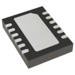 LTC2802CDE#TRPBF

LTC2802CDE#TRPBF is listed in the Drivers, Receivers, Transceivers range at ChipApex. The manufacturer field lists Analog Devices Inc.. Its product description is IC TRANSCEIVER…
Read More
LTC2802CDE#TRPBF is listed in the Drivers, Receivers, Transceivers range at ChipApex. The manufacturer field lists Analog Devices Inc.. Its product description is IC TRANSCEIVER…
Read More
LTC2802CDE#TRPBF is listed in the Drivers, Receivers, Transceivers range at ChipApex. The manufacturer field lists Analog Devices Inc.. Its product description is IC TRANSCEIVER…
Read More
LTC2802CDE#TRPBF is listed in the Drivers, Receivers, Transceivers range at ChipApex. The manufacturer field lists Analog Devices Inc.. Its product description is IC TRANSCEIVER…
Read More
Find out when a bare shock switch needs a pull resistor, when an MCU internal pull-up is enough, and why sensor modules and piezo…
Read More
LTC2802CDE#TRPBF is listed in the Drivers, Receivers, Transceivers range at ChipApex. The manufacturer field lists Analog Devices Inc.. Its product description is IC TRANSCEIVER…
Read More
LTC2802CDE#TRPBF is listed in the Drivers, Receivers, Transceivers range at ChipApex. The manufacturer field lists Analog Devices Inc.. Its product description is IC TRANSCEIVER…
Read More
LTC2802CDE#TRPBF is listed in the Drivers, Receivers, Transceivers range at ChipApex. The manufacturer field lists Analog Devices Inc.. Its product description is IC TRANSCEIVER…
Read More
LTC2802CDE#TRPBF is listed in the Drivers, Receivers, Transceivers range at ChipApex. The manufacturer field lists Analog Devices Inc.. Its product description is IC TRANSCEIVER…
Read More
Compare RC, crystal and MEMS oscillator circuits. Check ppm, jitter, load capacitance, startup margin and output compatibility before choosing a clock source.
Read More
LTC2802CDE#TRPBF is listed in the Drivers, Receivers, Transceivers range at ChipApex. The manufacturer field lists Analog Devices Inc.. Its product description is IC TRANSCEIVER…
Read More
LTC2802CDE#TRPBF is listed in the Drivers, Receivers, Transceivers range at ChipApex. The manufacturer field lists Analog Devices Inc.. Its product description is IC TRANSCEIVER…
Read More
The activity of extra discounts on wholesale prices is in full swing…
Please fill in your contact information and we will send you the latest wholesale price list.





