 ChipApex | Global Electronic Components Supplier
MC74LVX50DR2
Search Product
Search Post
— IC芯片 | 连接器 | 传感器 | 被动器件 —
Search productSearch post
— IC芯片 | 连接器 | 传感器 | 被动器件 —
Consult the customer manager about the wholesale price.
consultation hotline:86-132-6715-2157
email:[email protected]
Contact the product manager for consultation. One-stop consultation is available.
Do you want a lower wholesale price? Please send us your inquiry and we will reply immediately.
The MC74LVX50DR2G is a hex buffer fabricated with advanced high-speed CMOS technology. It operates within a supply voltage range of 2.0 V to 3.6 V. The device features inputs that tolerate voltages up to 6.5 V, enabling interface between 5.0 V and 3.0 V systems. Typical propagation delay is 4.1 ns at VCC = 3.3 V. Quiescent supply current is maximized at 2 µA at 25°C. Output noise immunity is defined by VNIH and VNIL at 28% VCC. Maximum dynamic VOLP is 0.5 V.
Verify the ordering suffix DR2G corresponds to the SOIC-14 package with tape and reel shipping configuration. Confirm RoHS compliance and lead-free status via the marking diagram or official distributor documentation. Ensure the part number matches the specific device code LVX50. Check datasheet revision date for latest electrical characteristics.
Select this component when hex buffering is required with 3.3 V operation. Consider input voltage tolerance if interfacing with 5 V sources. Evaluate propagation delay requirements against the typical 4.1 ns specification. Verify operating temperature range meets application needs from -40°C to 85°C. Assess power dissipation constraints relative to quiescent current specifications.
This device belongs to the MC74LVX50 family of hex buffers. It utilizes silicon gate CMOS technology for high-speed operation. The family includes variants with different packaging options such as TSSOP-14. The product line emphasizes low power consumption and high noise immunity for modern digital applications.
MC74LVX50DTG (TSSOP-14 rail), MC74LVX50DTR2G (TSSOP-14 tape and reel). Verify pinout compatibility and electrical parameters before substitution.
The inputs tolerate DC voltages up to 6.5 V.
Yes, the MC74LVX50 includes power down protection on its inputs.
The typical propagation delay is 4.1 ns at VCC = 3.3 V with CL = 15 pF.
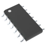 MC74LVX50DR2
The activity of extra discounts on wholesale prices is in full swing…
Please fill in your contact information and we will send you the latest wholesale price list.





