ChipApex | Global Electronic Components Supplier

SEARCH
Search Product
Search Post
— IC芯片 | 连接器 | 传感器 | 被动器件 —
Search productSearch post
— IC芯片 | 连接器 | 传感器 | 被动器件 —
Consult the customer manager about the wholesale price.
consultation hotline:86-132-6715-2157
email:[email protected]
Contact the product manager for consultation. One-stop consultation is available.
Do you want a lower wholesale price? Please send us your inquiry and we will reply immediately.
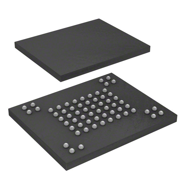
MX30LF2G28AD-XKI is listed in the Memory IC range at ChipApex. The manufacturer field lists Macronix. Its product description is IC FLASH 2GBIT PARALLEL 63VFBGA. Review the specifications below when checking this part for your BOM.
The MX30LF2G28AD-XKI is a 2Gb SLC NAND Flash memory device manufactured by Macronix. It features an x8 data bus width and operates within a voltage range of 2.7V to 3.6V. The device utilizes a 63-ball VFBGA package with dimensions of 9mm x 11mm. It supports ONFI 1.0 compliance and includes cache read capabilities for fast access. The memory array is organized into two planes, each containing 1024 blocks. Page size is 2048 bytes with 128-byte spare area, while block size is 128K bytes with 8K spare area.
Verify the specific ordering suffix XKI corresponds to the 63-ball VFBGA package and Industrial temperature grade (-40°C to +85°C). Confirm that the D suffix indicates the generation and 28A denotes the x8 mode A configuration. Ensure compatibility with host ECC requirements of 8-bit per (512+32) Byte as specified in the datasheet.
Select this component for designs requiring 2Gb capacity with x8 interface and single voltage operation. Consider the two-plane feature if parallel processing speed is needed. Verify that the 63-VFBGA package fits the PCB layout constraints. Check if the ONFI 1.0 compliance meets the controller's interface standards.
This part belongs to the MX30LFxG28AD family, which also includes 1Gb and 4Gb variants. All members share similar electrical characteristics and command sets but differ in density and page/block sizes. The XKI suffix specifically identifies the VFBGA package option within this series.
MX30LF1G28AD-XKI offers 1Gb capacity with identical package and interface. MX30LF4G28AD-XKI provides 4Gb capacity with the same form factor. Both are direct pin-compatible alternatives within the same product family.
Block protection is enabled by connecting the PT pin high at power-on, which protects the entire chip. Temporary or solid protection can be configured via BP bits using the Set Feature command.
Cache Read allows first-byte read-access latency of 25us and sequential read of 20ns. The internal buffer preloads the next page during the current read cycle to reduce subsequent access times.
Explore related parts through Memory, Integrated Circuits (ICs), all product categories, ChipApex homepage.
 MX30LF2G28AD-XKI
MX30LF2G28AD-XKI is listed in the Memory IC range at ChipApex. The manufacturer field lists Macronix. Its product description is IC FLASH 2GBIT PARALLEL 63VFBGA.…
Read More
Learn what an IMU measures, how accelerometers and gyroscopes work together, why orientation estimates drift, and what to compare.
Read More
Choose LED drivers by current, string voltage, dimming and thermal limits. Understand constant-current operation and the checks needed for your load.
Read More
Choose a rocker switch by AC/DC ratings, contact arrangement, illumination, panel fit and sealing. Get practical checks for engineering and component sourcing.
Read More
MX30LF2G28AD-XKI is listed in the Memory IC range at ChipApex. The manufacturer field lists Macronix. Its product description is IC FLASH 2GBIT PARALLEL 63VFBGA.…
Read MoreMX30LF2G28AD-XKI is listed in the Memory IC range at ChipApex. The manufacturer field lists Macronix. Its product description is IC FLASH 2GBIT PARALLEL 63VFBGA.…
Read More
Choose an AC to DC converter by input range, output demand, isolation, efficiency and thermal derating. Compare architectures and check installation needs.
Read More
See how a MEMS gyroscope measures angular rate, why its angle estimate drifts, and which range, noise, interface and temperature specs to compare.
Read More
MX30LF2G28AD-XKI is listed in the Memory IC range at ChipApex. The manufacturer field lists Macronix. Its product description is IC FLASH 2GBIT PARALLEL 63VFBGA.…
Read More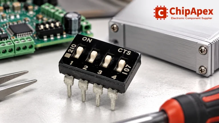
Choose a DIP switch by contact type, coded positions, footprint and signal ratings. Check logic polarity, assembly conditions and PCB configuration behavior.
Read More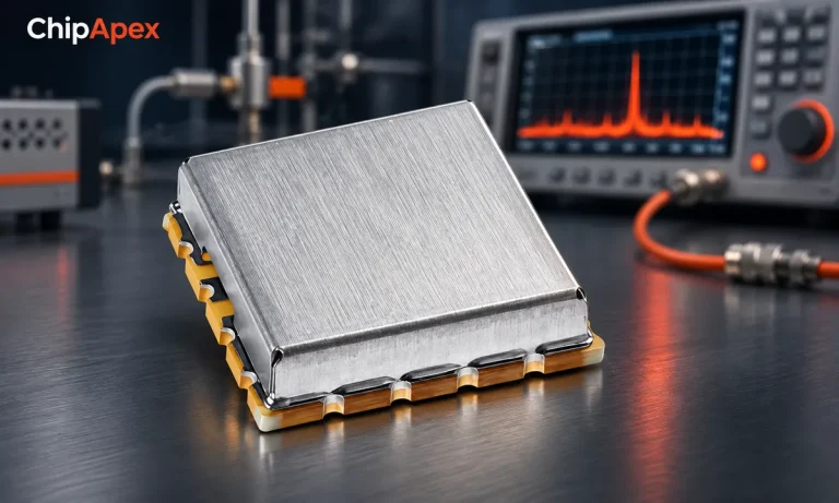
Understand voltage controlled oscillator tuning, phase noise and PLL operation. Check supply noise, output loading and requirements before selection.
Read More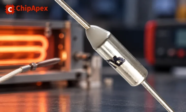
Understand thermal fuse operation, Tf, Th and Tm, electrical ratings and mounting. Check temperature limits and replacement requirements for your design.
Read More
The activity of extra discounts on wholesale prices is in full swing…
Please fill in your contact information and we will send you the latest wholesale price list.