 ChipApex | Global Electronic Components Supplier

SEARCH
Search Product
Search Post
— IC芯片 | 连接器 | 传感器 | 被动器件 —
Search productSearch post
— IC芯片 | 连接器 | 传感器 | 被动器件 —
Consult the customer manager about the wholesale price.
consultation hotline:86-132-6715-2157
email:[email protected]
Contact the product manager for consultation. One-stop consultation is available.
Do you want a lower wholesale price? Please send us your inquiry and we will reply immediately.
NLX2G17AMUTCG is listed in the Buffers, Drivers, Receivers, Transceivers range at ChipApex. The manufacturer field lists onsemi. Its product description is IC LOGIC SMD. Review the specifications below when checking this part for your BOM.
The NLX2G17AMUTCG is a dual non-inverting Schmitt-trigger buffer manufactured by onsemi using advanced high-speed CMOS technology. It operates within a supply voltage range of 1.65 V to 5.5 V and features overvoltage tolerant (OVT) input and output pins capable of withstanding voltages up to 7.0 V regardless of the supply level. The device provides balanced propagation delays, typically 3.1 ns at 5.0 V, and offers 24 mA balanced output source and sink capability. It is housed in an ultra-small UDFN6 package (CASE 517AQ, 1.45 x 1.0 mm footprint).
Verify the specific ordering suffix AMUTCG corresponds to the UDFN6 1.45 x 1.0 mm package (CASE 517AQ) as listed in the official datasheet. Confirm RoHS compliance and lead-free status directly from the manufacturer's documentation before procurement. Ensure design compatibility with the specified operating temperature range of -55°C to +125°C.
Select this component when a dual Schmitt-trigger buffer is required for signals with slow rise/fall times or high noise environments. The OVT feature allows interfacing with higher voltage lines without external protection. Consider the UDFN6 package dimensions for PCB layout constraints. Verify that the 1.65 V to 5.5 V supply range matches the system requirements.
This part belongs to the NLX2G17 MiniGate family of dual Schmitt-trigger buffers. The family includes variants with different package footprints such as ULLGA6 and other UDFN6 sizes. All variants share the same core electrical characteristics and functionality, differing primarily in physical package dimensions and pin pitch.
Consult the onsemi cross-reference tool for compatible alternatives from other manufacturers. Verify functional equivalence regarding Schmitt trigger thresholds and OVT capabilities. Check package compatibility if replacing in an existing design.
The input and output pins are overvoltage tolerant and can withstand voltages up to 7.0 V, regardless of the supply voltage.
No, the NLX2G17AMUTCG consists of dual non-inverting buffers.
Explore related parts through Logic, Integrated Circuits (ICs), all product categories, ChipApex homepage.
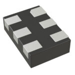 NLX2G17AMUTCG
Understand UART protocol framing, baud rate and electrical interfaces. Learn 8N1 timing, TX/RX wiring, buffering and practical troubleshooting steps.
Read More
NLX2G17AMUTCG is listed in the Buffers, Drivers, Receivers, Transceivers range at ChipApex. The manufacturer field lists onsemi. Its product description is IC LOGIC SMD.…
Read More
NLX2G17AMUTCG is listed in the Buffers, Drivers, Receivers, Transceivers range at ChipApex. The manufacturer field lists onsemi. Its product description is IC LOGIC SMD.…
Read More
Choose an AC to DC converter by input range, output demand, isolation, efficiency and thermal derating. Compare architectures and check installation needs.
Read More
Learn how a pressure transducer converts pressure into voltage, current, or digital output, and compare pressure references and key selection specs.
Read More
NLX2G17AMUTCG is listed in the Buffers, Drivers, Receivers, Transceivers range at ChipApex. The manufacturer field lists onsemi. Its product description is IC LOGIC SMD.…
Read More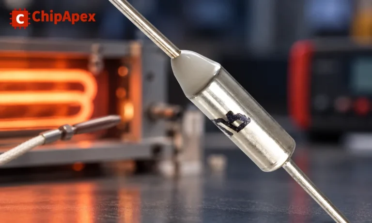
Understand thermal fuse operation, Tf, Th and Tm, electrical ratings and mounting. Check temperature limits and replacement requirements for your design.
Read More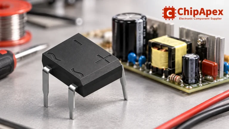
Select a bridge rectifier by reverse voltage, capacitor charging current, startup surge and cooling. Work through a stated DC voltage and ripple example.
Read More
NLX2G17AMUTCG is listed in the Buffers, Drivers, Receivers, Transceivers range at ChipApex. The manufacturer field lists onsemi. Its product description is IC LOGIC SMD.…
Read More
NLX2G17AMUTCG is listed in the Buffers, Drivers, Receivers, Transceivers range at ChipApex. The manufacturer field lists onsemi. Its product description is IC LOGIC SMD.…
Read More
NLX2G17AMUTCG is listed in the Buffers, Drivers, Receivers, Transceivers range at ChipApex. The manufacturer field lists onsemi. Its product description is IC LOGIC SMD.…
Read More
NLX2G17AMUTCG is listed in the Buffers, Drivers, Receivers, Transceivers range at ChipApex. The manufacturer field lists onsemi. Its product description is IC LOGIC SMD.…
Read More
The activity of extra discounts on wholesale prices is in full swing…
Please fill in your contact information and we will send you the latest wholesale price list.





