 ChipApex | Global Electronic Components Supplier

SEARCH
Search Product
Search Post
— IC芯片 | 连接器 | 传感器 | 被动器件 —
Search productSearch post
— IC芯片 | 连接器 | 传感器 | 被动器件 —
Consult the customer manager about the wholesale price.
consultation hotline:86-132-6715-2157
email:[email protected]
Contact the product manager for consultation. One-stop consultation is available.
Do you want a lower wholesale price? Please send us your inquiry and we will reply immediately.
OR2C10A3S208I-DB is listed in the Field Programmable Gate Array range at ChipApex. The manufacturer field lists Lattice Semiconductor Corporation. Its product description is FPGA, 256 CLBS, 12300 GATES. Review the specifications below when checking this part for your BOM.
The OR2C10A3S208I-DB is a Field Programmable Gate Array (FPGA) manufactured by Lattice Semiconductor. It features 256 Configurable Logic Blocks (CLBs), providing an equivalent gate count of 12,300 and 400 logic units. The device supports up to 152 I/O lines within a 208-pin TQFP package. It operates with a maximum clock frequency of 66.7 MHz and a typical combinational delay of 2.8 ns. The component is designed for industrial temperature ranges (-40°C to 85°C).
Verify the specific suffix 'DB' against official Lattice documentation to confirm packaging or environmental compliance details. Ensure the part number matches the exact pinout and voltage requirements for your design. Cross-reference with authorized distributors to confirm current availability and authenticity. Request full datasheets to validate electrical characteristics before integration.
Select this model when high I/O counts are required in a QFP form factor. Compare CLB density against smaller variants if resource constraints exist. Verify that the 66.7 MHz speed grade meets system timing requirements. Consider the industrial temperature range suitability for your specific deployment environment.
This component belongs to the OR2C series of FPGAs from Lattice Semiconductor. The series offers scalable logic resources for embedded control applications. The 208-pin package provides a balance between pin count and physical footprint. It serves as a bridge between simple PLDs and larger FPGA families.
Check for direct pin-to-pin replacements within the same OR2C family. Verify compatibility with existing toolchains and programming interfaces. Evaluate alternative packages if space constraints change. Confirm that performance metrics remain sufficient for the target application.
Explore related parts through Embedded, Integrated Circuits (ICs), all product categories, ChipApex homepage.
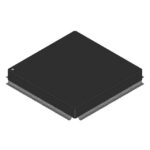 OR2C10A3S208I-DB

OR2C10A3S208I-DB is listed in the Field Programmable Gate Array range at ChipApex. The manufacturer field lists Lattice Semiconductor Corporation. Its product description is FPGA,…
Read More
OR2C10A3S208I-DB is listed in the Field Programmable Gate Array range at ChipApex. The manufacturer field lists Lattice Semiconductor Corporation. Its product description is FPGA,…
Read More
OR2C10A3S208I-DB is listed in the Field Programmable Gate Array range at ChipApex. The manufacturer field lists Lattice Semiconductor Corporation. Its product description is FPGA,…
Read More
Learn how a diode conducts, how to identify anode and cathode, and when to choose rectifier, TVS, Zener or photodiode types for a circuit.
Read More
OR2C10A3S208I-DB is listed in the Field Programmable Gate Array range at ChipApex. The manufacturer field lists Lattice Semiconductor Corporation. Its product description is FPGA,…
Read More
OR2C10A3S208I-DB is listed in the Field Programmable Gate Array range at ChipApex. The manufacturer field lists Lattice Semiconductor Corporation. Its product description is FPGA,…
Read More
OR2C10A3S208I-DB is listed in the Field Programmable Gate Array range at ChipApex. The manufacturer field lists Lattice Semiconductor Corporation. Its product description is FPGA,…
Read More
Choose a DIP switch by contact type, coded positions, footprint and signal ratings. Check logic polarity, assembly conditions and PCB configuration behavior.
Read More
OR2C10A3S208I-DB is listed in the Field Programmable Gate Array range at ChipApex. The manufacturer field lists Lattice Semiconductor Corporation. Its product description is FPGA,…
Read More
OR2C10A3S208I-DB is listed in the Field Programmable Gate Array range at ChipApex. The manufacturer field lists Lattice Semiconductor Corporation. Its product description is FPGA,…
Read More
Compare Pt100 and Pt1000 RTDs, two-, three- and four-wire connections, excitation and self-heating. Build an error budget from element to reported temperature.
Read More
OR2C10A3S208I-DB is listed in the Field Programmable Gate Array range at ChipApex. The manufacturer field lists Lattice Semiconductor Corporation. Its product description is FPGA,…
Read More
The activity of extra discounts on wholesale prices is in full swing…
Please fill in your contact information and we will send you the latest wholesale price list.






