 ChipApex | Global Electronic Components Supplier

SEARCH
Search Product
Search Post
— IC芯片 | 连接器 | 传感器 | 被动器件 —
Search productSearch post
— IC芯片 | 连接器 | 传感器 | 被动器件 —
Consult the customer manager about the wholesale price.
consultation hotline:86-132-6715-2157
email:[email protected]
Contact the product manager for consultation. One-stop consultation is available.
Do you want a lower wholesale price? Please send us your inquiry and we will reply immediately.
PI6C49CB01Q2WEX is listed in the Clock Buffers, Drivers range at ChipApex. The manufacturer field lists Diodes Incorporated. Its product description is IC CLK TRANSLTR 1:1 360MHZ 8SOIC. Review the specifications below when checking this part for your BOM.
The PI6C49CB01Q2WEX is a 1-to-1 differential-to-LVCMOS/LVTTL translator buffer manufactured by Diodes Incorporated. It accepts differential inputs including LVPECL, LVDS, LVHSTL, SSTL, and HCSL, converting them to a single-ended LVCMOS or LVTTL output. The device operates on a supply voltage ranging from 2.375 V to 3.465 V and supports maximum output frequencies up to 360 MHz. Propagation delay is specified at a maximum of 2.5 ns for 2.5 V operation and 2.0 ns for 3.3 V operation. It features part-to-part skew of 500 ps maximum and additive phase jitter as low as 0.09 ps RMS. The component is housed in an 8-pin SOIC (W) package and is qualified under AEC-Q100 standards.
Verify that the ordering suffix '2' corresponds to the Automotive Grade 2 temperature range (-40°C to 105°C). Confirm the 'WEX' suffix indicates the 8-pin SOIC package and Tape/Reel packaging format. Ensure compliance with RoHS and Halogen-free requirements if specified for the target assembly process.
Select this component when a single differential input must be translated to a single LVCMOS or LVTTL output. The PI6C49CB01Q2WEX is suitable for designs requiring AEC-Q100 Grade 2 qualification. For Grade 3 qualification (-40°C to 85°C), the PI6C49CB01Q3WEX variant should be considered instead.
This part belongs to the PI6C49CB01Q family of differential translators. The specific suffix '2' denotes the Automotive Grade 2 temperature rating. Other variants in the series include the Q3 suffix for Grade 3 ratings. The device is distinct from multi-output buffers like the PI6C49CB02Q series.
The PI6C49CB01Q3WEX serves as a direct replacement for applications requiring the lower Automotive Grade 3 temperature range (-40°C to 85°C). Verify thermal requirements before substituting.
The CLK/nCLK input pair accepts LVPECL, LVDS, LVHSTL, SSTL, and HCSL levels.
The maximum output frequency is 360 MHz.
At 2.5V, the maximum propagation delay is 2.5 ns. At 3.3V, it decreases to a maximum of 2.0 ns.
Explore related parts through Clock/Timing, Integrated Circuits (ICs), all product categories, ChipApex homepage.
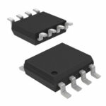 PI6C49CB01Q2WEX

PI6C49CB01Q2WEX is listed in the Clock Buffers, Drivers range at ChipApex. The manufacturer field lists Diodes Incorporated. Its product description is IC CLK TRANSLTR…
Read More
Understand tactile switches, PCB and keyboard differences, four-pin wiring, debounce, force, travel and replacement checks for reliable control inputs.
Read More
Select a bridge rectifier by reverse voltage, capacitor charging current, startup surge and cooling. Work through a stated DC voltage and ripple example.
Read More
Learn what an IMU measures, how accelerometers and gyroscopes work together, why orientation estimates drift, and what to compare.
Read More
Select MOV varistors by continuous voltage, clamping behavior, surge waveform and repetition. Check thermal disconnection, fuse coordination and replacements.
Read More
PI6C49CB01Q2WEX is listed in the Clock Buffers, Drivers range at ChipApex. The manufacturer field lists Diodes Incorporated. Its product description is IC CLK TRANSLTR…
Read More
PI6C49CB01Q2WEX is listed in the Clock Buffers, Drivers range at ChipApex. The manufacturer field lists Diodes Incorporated. Its product description is IC CLK TRANSLTR…
Read More
PI6C49CB01Q2WEX is listed in the Clock Buffers, Drivers range at ChipApex. The manufacturer field lists Diodes Incorporated. Its product description is IC CLK TRANSLTR…
Read More
PI6C49CB01Q2WEX is listed in the Clock Buffers, Drivers range at ChipApex. The manufacturer field lists Diodes Incorporated. Its product description is IC CLK TRANSLTR…
Read More
PI6C49CB01Q2WEX is listed in the Clock Buffers, Drivers range at ChipApex. The manufacturer field lists Diodes Incorporated. Its product description is IC CLK TRANSLTR…
Read More
PI6C49CB01Q2WEX is listed in the Clock Buffers, Drivers range at ChipApex. The manufacturer field lists Diodes Incorporated. Its product description is IC CLK TRANSLTR…
Read More
Learn how a diode conducts, how to identify anode and cathode, and when to choose rectifier, TVS, Zener or photodiode types for a circuit.
Read More
The activity of extra discounts on wholesale prices is in full swing…
Please fill in your contact information and we will send you the latest wholesale price list.






