 ChipApex | Global Electronic Components Supplier

SEARCH
Search Product
Search Post
— IC芯片 | 连接器 | 传感器 | 被动器件 —
Search productSearch post
— IC芯片 | 连接器 | 传感器 | 被动器件 —
Consult the customer manager about the wholesale price.
consultation hotline:86-132-6715-2157
email:[email protected]
Contact the product manager for consultation. One-stop consultation is available.
Do you want a lower wholesale price? Please send us your inquiry and we will reply immediately.
PI6C49S1510ZDIE is listed in the Clock Buffers, Drivers range at ChipApex. The manufacturer field lists Diodes Incorporated. Its product description is IC CLK BUFFER 3:11 1.5GHZ 48TQFN. Review the specifications below when checking this part for your BOM.
The PI6C49S1510ZDIE is a high-performance fanout buffer from Diodes Incorporated, housed in a 48-pin TQFN package. It supports differential output frequencies up to 1.5 GHz and features ten outputs divided into two banks. Each bank allows user-configurable signaling standards including LVDS, LVPECL, or HCSL via pin selection. The device includes an LVCMOS reference output capable of reaching 200 MHz. Key electrical parameters include a maximum propagation delay of 2.2 ns, a typical additive phase jitter of less than 0.03 ps at 156.25 MHz (12 kHz to 20 MHz range), and operation within a supply voltage range of 2.375 V to 3.465 V.
Verify the ordering suffix 'E' confirms Pb-free and Green compliance for the PI6C49S1510ZDIE variant. Confirm the 'X' suffix indicates tape and reel packaging if required for automated assembly. Ensure the operating temperature range of -40 °C to +85 °C aligns with system thermal requirements. Cross-reference the 48-pin TQFN mechanical dimensions against the PCB footprint design.
Select this component when distributing clocks up to 1.5 GHz with mixed interface requirements across different destination devices. The dual-bank architecture allows independent configuration of output standards, simplifying board layouts where LVDS and LVPECL loads coexist. Verify that the power supply filtering meets the recommended isolation guidelines to maintain the specified ultra-low jitter performance.
This part belongs to the PI6C49S1510A series of high-performance differential fanout buffers. It is functionally equivalent to the PI6C49S1510 but packaged in the ZD (TQFN-48) format. The device utilizes proprietary input detection techniques to ensure robust operation by reflecting illegal input states through the output pins.
The PI6C49S1510ZDIEX serves as the tape and reel version of the same functional device. Other members of the PI6C49S1510 family may offer different pin counts or package styles but share similar core specifications.
The signaling standard for each bank (Bank A and Bank B) is selected using the OPMODEA and OPMODEB pins. These pins support LVCMOS/LVTTL levels to select between LVPECL, LVDS, or HCSL modes.
The LVCMOS reference output (Ref_Out) supports frequencies up to 200 MHz when driven by a reference input, or up to 50 MHz when driven by a crystal oscillator.
The PI6C49S1510 integrates a detection technique that identifies illegal input states, such as open inputs or both inputs being high/low. In these cases, the output status is forced to Logic Low.
Explore related parts through Clock/Timing, Integrated Circuits (ICs), all product categories, ChipApex homepage.
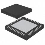 PI6C49S1510ZDIE
 is listed in the Clock Buffers, Drivers range at ChipApex. The manufacturer field lists Diodes Incorporated. Its product description is IC CLK BUFFER…
Read More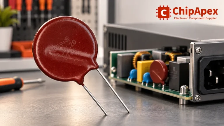
Select MOV varistors by continuous voltage, clamping behavior, surge waveform and repetition. Check thermal disconnection, fuse coordination and replacements.
Read More
PI6C49S1510ZDIE is listed in the Clock Buffers, Drivers range at ChipApex. The manufacturer field lists Diodes Incorporated. Its product description is IC CLK BUFFER…
Read More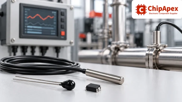
Compare thermistors, RTDs, thermocouples and temperature ICs. Learn how range, accuracy, response, interfaces and mounting affect component selection.
Read More
PI6C49S1510ZDIE is listed in the Clock Buffers, Drivers range at ChipApex. The manufacturer field lists Diodes Incorporated. Its product description is IC CLK BUFFER…
Read More
PI6C49S1510ZDIE is listed in the Clock Buffers, Drivers range at ChipApex. The manufacturer field lists Diodes Incorporated. Its product description is IC CLK BUFFER…
Read More
PI6C49S1510ZDIE is listed in the Clock Buffers, Drivers range at ChipApex. The manufacturer field lists Diodes Incorporated. Its product description is IC CLK BUFFER…
Read More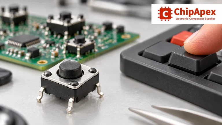
Understand tactile switches, PCB and keyboard differences, four-pin wiring, debounce, force, travel and replacement checks for reliable control inputs.
Read More
PI6C49S1510ZDIE is listed in the Clock Buffers, Drivers range at ChipApex. The manufacturer field lists Diodes Incorporated. Its product description is IC CLK BUFFER…
Read More
PI6C49S1510ZDIE is listed in the Clock Buffers, Drivers range at ChipApex. The manufacturer field lists Diodes Incorporated. Its product description is IC CLK BUFFER…
Read More
PI6C49S1510ZDIE is listed in the Clock Buffers, Drivers range at ChipApex. The manufacturer field lists Diodes Incorporated. Its product description is IC CLK BUFFER…
Read More
PI6C49S1510ZDIE is listed in the Clock Buffers, Drivers range at ChipApex. The manufacturer field lists Diodes Incorporated. Its product description is IC CLK BUFFER…
Read More
The activity of extra discounts on wholesale prices is in full swing…
Please fill in your contact information and we will send you the latest wholesale price list.




