 ChipApex | Global Electronic Components Supplier

SEARCH
Search Product
Search Post
— IC芯片 | 连接器 | 传感器 | 被动器件 —
Search productSearch post
— IC芯片 | 连接器 | 传感器 | 被动器件 —
Consult the customer manager about the wholesale price.
consultation hotline:86-132-6715-2157
email:[email protected]
Contact the product manager for consultation. One-stop consultation is available.
Do you want a lower wholesale price? Please send us your inquiry and we will reply immediately.
PI6CV855LE is listed in the Clock Generators, PLLs, Frequency Synthesizers range at ChipApex. The manufacturer field lists Diodes Incorporated. Its product description is IC PLL CLOCK DRIVER 28TSSOP. Review the specifications below when checking this part for your BOM.
The PI6CV855LE is a PLL-based clock driver designed for SSTL_2 DDR SDRAM applications. It operates with AVDD and VDDQ at 2.5V (range 2.3V to 2.7V). The device distributes one differential clock input pair (CLK, CLK) to five differential output pairs (Y0-Y4) and provides one differential feedback pair (FBOUT, FBOUT). Inputs and outputs utilize SSTL_2 levels. The maximum operating frequency is 167 MHz, with an application frequency up to 134 MHz. Key timing parameters include a maximum cycle-to-cycle jitter of 57 ps, period jitter of 57 ps, and half-period jitter of 101 ps. Input/output slew rates are between 0.2 and 1.0 V/ns. The component is housed in a 28-pin TSSOP package.
Verify the specific ordering suffix 'LE' corresponds to the Pb-free and Green packaging variant as documented in the datasheet. Confirm that the 28-pin TSSOP physical dimensions match the target PCB footprint requirements. Ensure supply chain sources provide original manufacturer documentation to validate the component's authenticity and compliance status.
Select this component when designing SSTL_2 compliant DDR memory interfaces requiring a single differential input to drive multiple loads. The device supports frequencies up to 167 MHz. Consider the 28-pin TSSOP package constraints. Verify that the system power supplies can maintain the required 2.5V range for both analog and I/O sections.
This part belongs to the PI6CV855 series of PLL clock drivers manufactured by Diodes Incorporated. It is specifically engineered for memory applications using SSTL_2 signaling standards. The LE suffix indicates the lead-free and environmentally friendly packaging configuration available for this specific model.
Public confirmed substitute part numbers are not provided in the source material.
The PLL is turned off and bypassed by strapping the Analog Power input (AVDD) low.
The maximum operating frequency is 167 MHz, while the application frequency meets all timing parameters up to 134 MHz.
Both the inputs (CLK, CLK, FBIN, FBIN) and outputs (Yx, Yx, FBOUT, FBOUT) operate at SSTL_2 levels.
Explore related parts through Clock/Timing, Integrated Circuits (ICs), all product categories, ChipApex homepage.
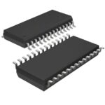 PI6CV855LE
PI6CV855LE is listed in the Clock Generators, PLLs, Frequency Synthesizers range at ChipApex. The manufacturer field lists Diodes Incorporated. Its product description is IC…
Read More
PI6CV855LE is listed in the Clock Generators, PLLs, Frequency Synthesizers range at ChipApex. The manufacturer field lists Diodes Incorporated. Its product description is IC…
Read More
PI6CV855LE is listed in the Clock Generators, PLLs, Frequency Synthesizers range at ChipApex. The manufacturer field lists Diodes Incorporated. Its product description is IC…
Read More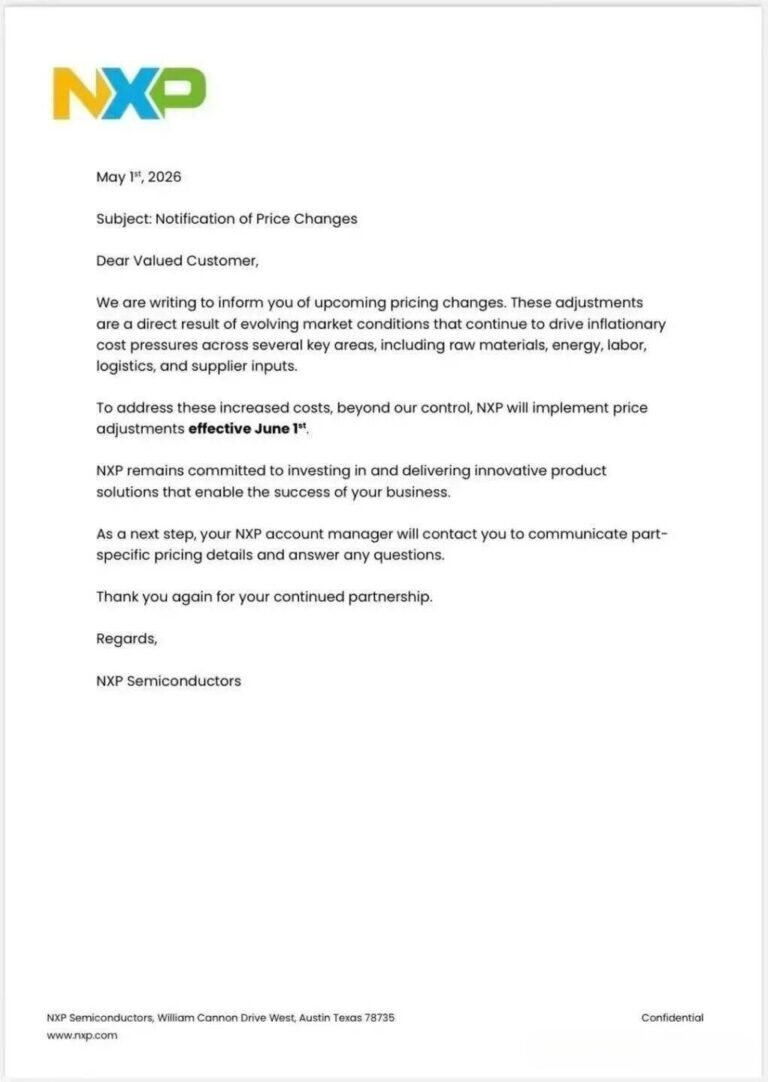
PI6CV855LE is listed in the Clock Generators, PLLs, Frequency Synthesizers range at ChipApex. The manufacturer field lists Diodes Incorporated. Its product description is IC…
Read More
PI6CV855LE is listed in the Clock Generators, PLLs, Frequency Synthesizers range at ChipApex. The manufacturer field lists Diodes Incorporated. Its product description is IC…
Read More
PI6CV855LE is listed in the Clock Generators, PLLs, Frequency Synthesizers range at ChipApex. The manufacturer field lists Diodes Incorporated. Its product description is IC…
Read More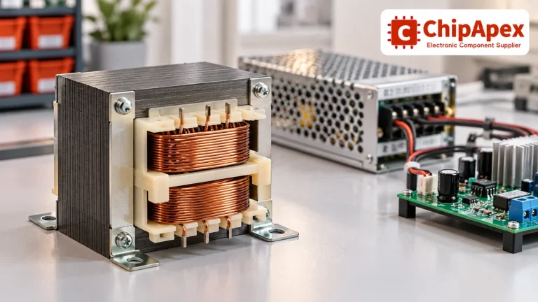
Select power transformers by input frequency, secondary VA, rectifier load, isolation, regulation and inrush. Build a clearer specification for your next RFQ.
Read More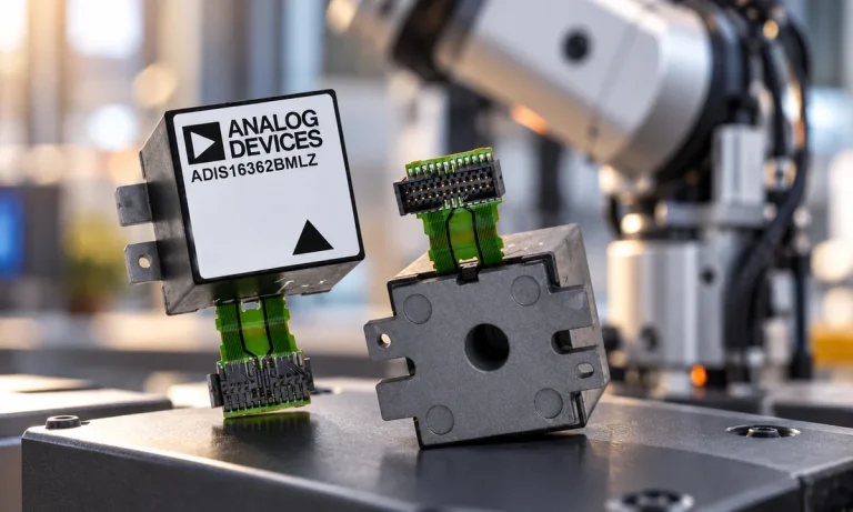
Learn what an IMU measures, how accelerometers and gyroscopes work together, why orientation estimates drift, and what to compare.
Read More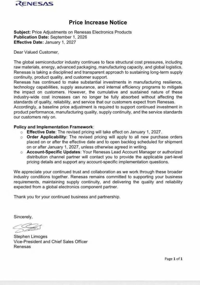
PI6CV855LE is listed in the Clock Generators, PLLs, Frequency Synthesizers range at ChipApex. The manufacturer field lists Diodes Incorporated. Its product description is IC…
Read More
PI6CV855LE is listed in the Clock Generators, PLLs, Frequency Synthesizers range at ChipApex. The manufacturer field lists Diodes Incorporated. Its product description is IC…
Read More
PI6CV855LE is listed in the Clock Generators, PLLs, Frequency Synthesizers range at ChipApex. The manufacturer field lists Diodes Incorporated. Its product description is IC…
Read MorePI6CV855LE is listed in the Clock Generators, PLLs, Frequency Synthesizers range at ChipApex. The manufacturer field lists Diodes Incorporated. Its product description is IC…
Read More
The activity of extra discounts on wholesale prices is in full swing…
Please fill in your contact information and we will send you the latest wholesale price list.





