 ChipApex | Global Electronic Components Supplier

SEARCH
Search Product
Search Post
— IC芯片 | 连接器 | 传感器 | 被动器件 —
Search productSearch post
— IC芯片 | 连接器 | 传感器 | 被动器件 —
Consult the customer manager about the wholesale price.
consultation hotline:86-132-6715-2157
email:[email protected]
Contact the product manager for consultation. One-stop consultation is available.
Do you want a lower wholesale price? Please send us your inquiry and we will reply immediately.
RC19102AGNT#KD0 is listed in the Clock Buffers, Drivers range at ChipApex. The manufacturer field lists Renesas Electronics Corporation. Its product description is RC19102A GEN6 1.8V BUFFER 2 O/P. Review the specifications below when checking this part for your BOM.
The RC19102AGNT#KD0 is a clock buffer from the Renesas RC19102A series, designed for high-speed serial applications. It features two outputs and supports input frequencies up to 400 MHz. The device operates within a supply voltage range of 2.97 V to 3.63 V and functions reliably across an extended temperature range of -40°C to +105°C. With a maximum propagation delay of 1.7 ns, it provides precise timing distribution for PCIe Gen6 compliant systems.
Verify the specific ordering suffix #KD0 against the manufacturer's current datasheet to confirm packaging details and availability status. Ensure compatibility with system power requirements before procurement.
Select this component when a low-jitter, two-output clock buffer is required for PCIe Gen6 designs. Confirm that the 3.3V core voltage aligns with the target board design and that the VFQFPN package fits the PCB layout constraints.
This part belongs to the RC192xx family of clock multiplexers and buffers. While similar to the RC19202, the RC19102A variant is specifically optimized as a buffer rather than a multiplexer, offering simplified signal routing for single-source clock distribution tasks in high-performance computing environments.
Check for direct pin-to-pin replacements within the RC191xx or RC192xx families. Verify if upgraded generations like the RC193xx offer backward compatibility without requiring schematic changes.
Explore related parts through Clock/Timing, Integrated Circuits (ICs), all product categories, ChipApex homepage.
 RC19102AGNT#KD0
RC19102AGNT#KD0 is listed in the Clock Buffers, Drivers range at ChipApex. The manufacturer field lists Renesas Electronics Corporation. Its product description is RC19102A GEN6…
Read More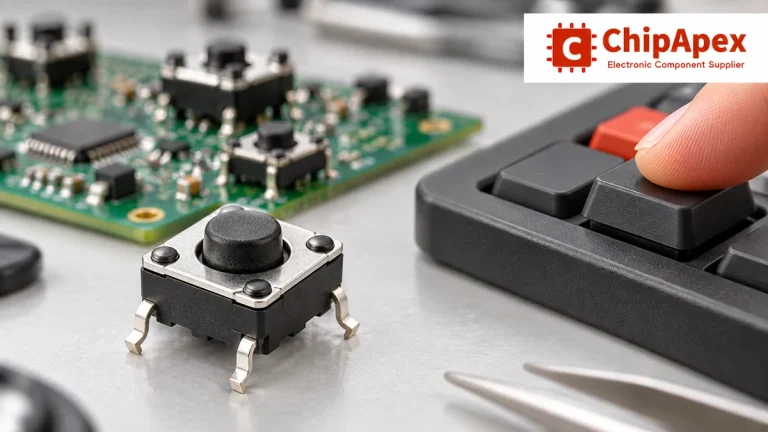
Choose tactile switches by operating force, travel, actuator height, footprint and lifetime. Check debounce, sealing and the assembled button mechanism.
Read More
RC19102AGNT#KD0 is listed in the Clock Buffers, Drivers range at ChipApex. The manufacturer field lists Renesas Electronics Corporation. Its product description is RC19102A GEN6…
Read More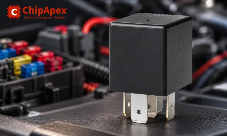
Learn the relay definition, coil and contact operation, NO and NC forms, load ratings and suppression choices. Compare mechanical, reed and solid-state types.
Read More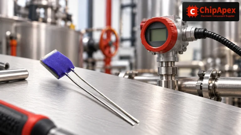
Compare Pt100 and Pt1000 RTDs, two-, three- and four-wire connections, excitation and self-heating. Build an error budget from element to reported temperature.
Read More
RC19102AGNT#KD0 is listed in the Clock Buffers, Drivers range at ChipApex. The manufacturer field lists Renesas Electronics Corporation. Its product description is RC19102A GEN6…
Read More
RC19102AGNT#KD0 is listed in the Clock Buffers, Drivers range at ChipApex. The manufacturer field lists Renesas Electronics Corporation. Its product description is RC19102A GEN6…
Read More
Find out when a bare shock switch needs a pull resistor, when an MCU internal pull-up is enough, and why sensor modules and piezo…
Read More
Select MOV varistors by continuous voltage, clamping behavior, surge waveform and repetition. Check thermal disconnection, fuse coordination and replacements.
Read More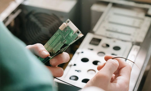
RC19102AGNT#KD0 is listed in the Clock Buffers, Drivers range at ChipApex. The manufacturer field lists Renesas Electronics Corporation. Its product description is RC19102A GEN6…
Read More
Choose an AC to DC converter by input range, output demand, isolation, efficiency and thermal derating. Compare architectures and check installation needs.
Read More
RC19102AGNT#KD0 is listed in the Clock Buffers, Drivers range at ChipApex. The manufacturer field lists Renesas Electronics Corporation. Its product description is RC19102A GEN6…
Read More
The activity of extra discounts on wholesale prices is in full swing…
Please fill in your contact information and we will send you the latest wholesale price list.




