ChipApex | Global Electronic Components Supplier

SEARCH
Search Product
Search Post
— IC芯片 | 连接器 | 传感器 | 被动器件 —
Search productSearch post
— IC芯片 | 连接器 | 传感器 | 被动器件 —
Consult the customer manager about the wholesale price.
consultation hotline:86-132-6715-2157
email:[email protected]
Contact the product manager for consultation. One-stop consultation is available.
Do you want a lower wholesale price? Please send us your inquiry and we will reply immediately.
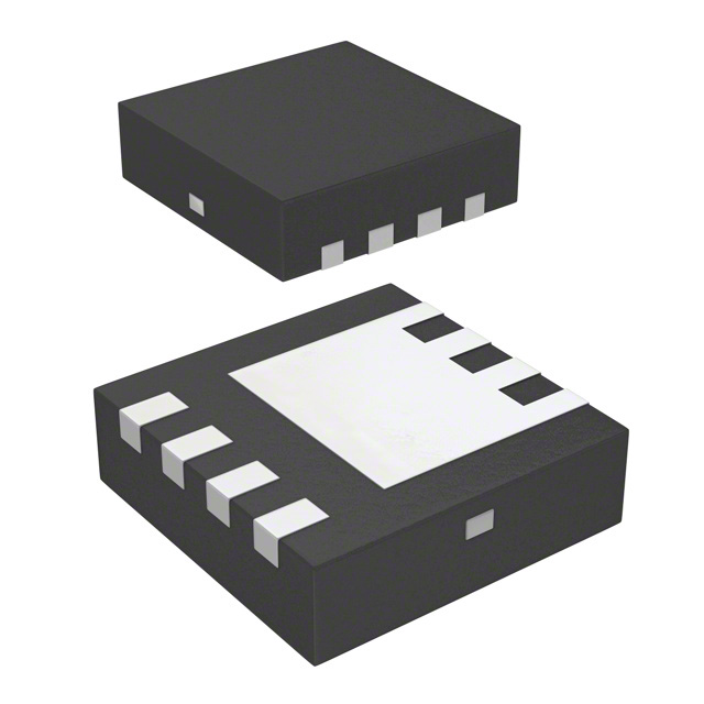
SISS5112DN-T1-GE3 is listed in the Single FETs, MOSFETs range at ChipApex. The manufacturer field lists Vishay Siliconix. Its product description is N-CHANNEL 100 V (D-S) MOSFET POW. Review the specifications below when checking this part for your BOM.
The SiSS5112DN is a Vishay Siliconix N-Channel MOSFET featuring TrenchFET Gen V technology. It offers a drain-source voltage of 100 V and a maximum on-resistance of 0.0149 Ω at VGS = 10 V. The device supports a continuous drain current of 40.7 A at TC = 25 °C. Typical gate charge is 8 nC at VGS = 7.5 V. It utilizes a PowerPAK 1212-8S leadless package with a junction-to-case thermal resistance of 1.9 °C/W typical.
Verify the specific ordering suffix -T1-GE3 to confirm lead-free and halogen-free compliance status as defined by Vishay material categorization standards. Ensure the PowerPAK 1212-8S package dimensions match your PCB footprint requirements, noting the exposed copper terminals require appropriate soldering profiles. Confirm that the application environment stays within the specified operating junction temperature range of -55 °C to +150 °C.
Select this component for applications requiring high efficiency in compact spaces due to its low thermal resistance and small PowerPAK 1212-8S footprint. Consider the 100 V rating and 40.7 A current capability for synchronous rectification or DC/DC converter designs. Evaluate the optimized figures-of-merit for switching performance needs. Validate thermal management strategies against the junction-to-ambient resistance values provided in the datasheet for your specific board layout.
This N-Channel MOSFET belongs to Vishay's TrenchFET Gen V family, designed for high-efficiency power switching. The PowerPAK 1212-8S package provides a compact solution suitable for space-constrained electronics. The device integrates advanced trench gate technology to minimize conduction and switching losses, making it suitable for modern power supply architectures requiring high power density.
Consult official Vishay documentation for verified cross-reference part numbers. Do not assume functional equivalence based solely on pinout or voltage ratings. Verify that any substitute component meets the specific RDS(on), Qg, and thermal performance requirements of the original design.
The maximum operating junction temperature is +150 °C.
Yes, the datasheet confirms that 100% of units are tested for unclamped inductive switching (UIS).
Explore related parts through FETs, MOSFETs, Transistors, Discrete Semiconductor Products, all product categories.
 SISS5112DN-T1-GE3

Learn what an IMU measures, how accelerometers and gyroscopes work together, why orientation estimates drift, and what to compare.
Read More
SISS5112DN-T1-GE3 is listed in the Single FETs, MOSFETs range at ChipApex. The manufacturer field lists Vishay Siliconix. Its product description is N-CHANNEL 100 V…
Read MoreSISS5112DN-T1-GE3 is listed in the Single FETs, MOSFETs range at ChipApex. The manufacturer field lists Vishay Siliconix. Its product description is N-CHANNEL 100 V…
Read More
SISS5112DN-T1-GE3 is listed in the Single FETs, MOSFETs range at ChipApex. The manufacturer field lists Vishay Siliconix. Its product description is N-CHANNEL 100 V…
Read More
SISS5112DN-T1-GE3 is listed in the Single FETs, MOSFETs range at ChipApex. The manufacturer field lists Vishay Siliconix. Its product description is N-CHANNEL 100 V…
Read More
SISS5112DN-T1-GE3 is listed in the Single FETs, MOSFETs range at ChipApex. The manufacturer field lists Vishay Siliconix. Its product description is N-CHANNEL 100 V…
Read More
SISS5112DN-T1-GE3 is listed in the Single FETs, MOSFETs range at ChipApex. The manufacturer field lists Vishay Siliconix. Its product description is N-CHANNEL 100 V…
Read More
SISS5112DN-T1-GE3 is listed in the Single FETs, MOSFETs range at ChipApex. The manufacturer field lists Vishay Siliconix. Its product description is N-CHANNEL 100 V…
Read More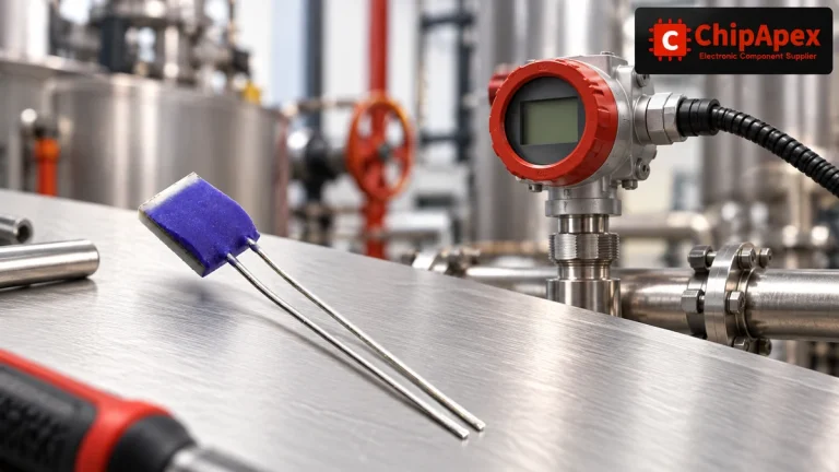
Compare Pt100 and Pt1000 RTDs, two-, three- and four-wire connections, excitation and self-heating. Build an error budget from element to reported temperature.
Read More
SISS5112DN-T1-GE3 is listed in the Single FETs, MOSFETs range at ChipApex. The manufacturer field lists Vishay Siliconix. Its product description is N-CHANNEL 100 V…
Read More
SISS5112DN-T1-GE3 is listed in the Single FETs, MOSFETs range at ChipApex. The manufacturer field lists Vishay Siliconix. Its product description is N-CHANNEL 100 V…
Read More
SISS5112DN-T1-GE3 is listed in the Single FETs, MOSFETs range at ChipApex. The manufacturer field lists Vishay Siliconix. Its product description is N-CHANNEL 100 V…
Read More
The activity of extra discounts on wholesale prices is in full swing…
Please fill in your contact information and we will send you the latest wholesale price list.