 ChipApex | Global Electronic Components Supplier

SEARCH
Search Product
Search Post
— IC芯片 | 连接器 | 传感器 | 被动器件 —
Search productSearch post
— IC芯片 | 连接器 | 传感器 | 被动器件 —
Consult the customer manager about the wholesale price.
consultation hotline:86-132-6715-2157
email:[email protected]
Contact the product manager for consultation. One-stop consultation is available.
Do you want a lower wholesale price? Please send us your inquiry and we will reply immediately.
SN74ABT5403DWR is listed in the Buffers, Drivers, Receivers, Transceivers range at ChipApex. The manufacturer field lists Texas Instruments. Its product description is IC BUFFER INVERT 5.5V 28SOIC. Review the specifications below when checking this part for your BOM.
The SN74ABT5403DWR is a 12-bit line and memory driver featuring three-state outputs, manufactured by Texas Instruments. It utilizes EPIC-IIB BiCMOS technology for reduced power dissipation. The device operates within a supply voltage range of 4.5 V to 5.5 V and supports an operating temperature range from -40°C to +85°C. Outputs are designed to source or sink up to 12 mA and include equivalent 25-ohm series resistors. Propagation delays typically range from 1.5 ns to 6.9 ns at VCC = 5 V with CL = 50 pF.
Verify the specific ordering suffix 'DWR' corresponds to the SOIC-28 package and tape-and-reel quantity of 1000 units. Confirm that the RoHS status and lead finish match project requirements. Ensure the component meets the specified industrial temperature range limits before finalizing procurement orders.
Select this component when designing systems requiring 12-bit data buffering with high-density integration. The internal series resistors simplify layout by reducing EMI. Verify that the 12 mA drive capability aligns with load requirements. Consider the dual enable inputs for complex bus arbitration logic compared to single-enable alternatives.
This part belongs to the SN54/74ABT5403 family of 12-bit line/memory drivers. While the SN54 variant covers military temperatures, the SN74 version is rated for industrial applications. The DW suffix specifically denotes the plastic small-outline package configuration used in surface-mount assemblies.
SN74ABT5403DW
To ensure the high-impedance state during power-up or power-down, the OE input should be tied to VCC through a pullup resistor. The minimum resistor value is determined by the current-sinking capability of the driver.
The 3-state control gate consists of two active-low inputs (OE1 and OE2) acting as a two-input AND gate. If either OE1 or OE2 is high, all 12 outputs enter the high-impedance state.
Explore related parts through Logic, Integrated Circuits (ICs), all product categories, ChipApex homepage.
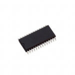 SN74ABT5403DWR
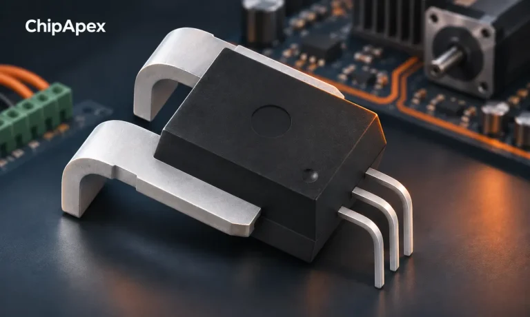
Compare Hall, shunt, current transformer and Rogowski sensing. Check AC/DC capability, accuracy, isolation, heat and response before selecting a sensor.
Read More
SN74ABT5403DWR is listed in the Buffers, Drivers, Receivers, Transceivers range at ChipApex. The manufacturer field lists Texas Instruments. Its product description is IC BUFFER…
Read More
SN74ABT5403DWR is listed in the Buffers, Drivers, Receivers, Transceivers range at ChipApex. The manufacturer field lists Texas Instruments. Its product description is IC BUFFER…
Read More
SN74ABT5403DWR is listed in the Buffers, Drivers, Receivers, Transceivers range at ChipApex. The manufacturer field lists Texas Instruments. Its product description is IC BUFFER…
Read More
SN74ABT5403DWR is listed in the Buffers, Drivers, Receivers, Transceivers range at ChipApex. The manufacturer field lists Texas Instruments. Its product description is IC BUFFER…
Read More
SN74ABT5403DWR is listed in the Buffers, Drivers, Receivers, Transceivers range at ChipApex. The manufacturer field lists Texas Instruments. Its product description is IC BUFFER…
Read More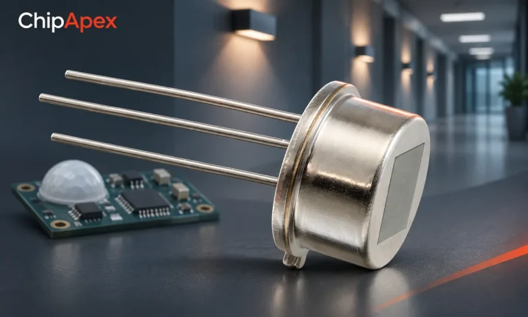
Understand how motion sensors work. Compare PIR, radar and ultrasonic sensing, then check presence detection, false triggers, optics and signal conditioning.
Read More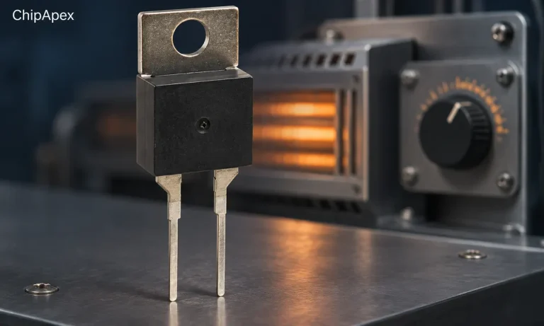
Learn how a thermostat in a heater works. Check hysteresis, reset mode, thermal placement and contact ratings before selecting a mechanical control.
Read More
SN74ABT5403DWR is listed in the Buffers, Drivers, Receivers, Transceivers range at ChipApex. The manufacturer field lists Texas Instruments. Its product description is IC BUFFER…
Read More
SN74ABT5403DWR is listed in the Buffers, Drivers, Receivers, Transceivers range at ChipApex. The manufacturer field lists Texas Instruments. Its product description is IC BUFFER…
Read More
SN74ABT5403DWR is listed in the Buffers, Drivers, Receivers, Transceivers range at ChipApex. The manufacturer field lists Texas Instruments. Its product description is IC BUFFER…
Read More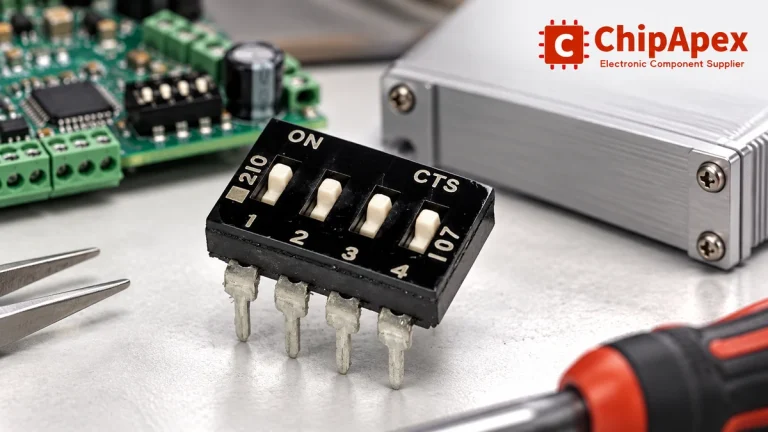
Choose a DIP switch by contact type, coded positions, footprint and signal ratings. Check logic polarity, assembly conditions and PCB configuration behavior.
Read More
The activity of extra discounts on wholesale prices is in full swing…
Please fill in your contact information and we will send you the latest wholesale price list.





