 ChipApex | Global Electronic Components Supplier

SEARCH
Search Product
Search Post
— IC芯片 | 连接器 | 传感器 | 被动器件 —
Search productSearch post
— IC芯片 | 连接器 | 传感器 | 被动器件 —
Consult the customer manager about the wholesale price.
consultation hotline:86-132-6715-2157
email:[email protected]
Contact the product manager for consultation. One-stop consultation is available.
Do you want a lower wholesale price? Please send us your inquiry and we will reply immediately.
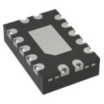
SN74AHCT125BQAR is listed in the Buffers, Drivers, Receivers, Transceivers range at ChipApex. The manufacturer field lists Texas Instruments. Its product description is 4-CH 4.5-V TO 5.5-V BUFFERS. Review the specifications below when checking this part for your BOM.
The SN74AHCT125BQAR is a commercial-grade quadruple bus buffer gate with 3-state outputs manufactured by Texas Instruments. It operates within a supply voltage range of 4.5 V to 5.5 V and supports an operating temperature range of -40°C to 85°C. The device features independent output enable controls for each channel, providing high-level output current of -8 mA and low-level output current of 8 mA. Propagation delays are specified at 6.5 ns maximum (CL = 15 pF) and 8.5 ns maximum (CL = 50 pF). It utilizes a WQFN-14 package.
Verify the specific BQA suffix corresponds to the WQFN-14 package configuration required for your PCB layout. Confirm that the commercial grade rating (-40°C to 85°C) aligns with your environmental specifications. Ensure input pins are terminated to VCC or GND if unused to prevent undefined operational states.
Select this component when TTL-compatible buffering with independent channel control is required in a compact surface-mount form factor. The AHCT technology provides CMOS speed with TTL input compatibility. Consider thermal impedance characteristics during design if multiple channels are actively driven simultaneously.
This part belongs to the SNx4AHCT125 family of quadruple bus buffer gates. The 'BQA' suffix specifically denotes the WQFN (Wide Quad Flat No-leads) 14-pin package variant. Other variants in the series include SOIC, SSOP, and PDIP packages, offering flexibility for different manufacturing and assembly requirements.
SN74AHCT125DR (SOIC-14)
When the output-enable (OE) input is high, the respective gate output enters a high-impedance state, effectively disconnecting it from the circuit.
All unused inputs must be held at VCC or GND to ensure proper device operation and prevent oscillations or excessive power consumption.
Explore related parts through Logic, Integrated Circuits (ICs), all product categories, ChipApex homepage.
 SN74AHCT125BQAR

SN74AHCT125BQAR is listed in the Buffers, Drivers, Receivers, Transceivers range at ChipApex. The manufacturer field lists Texas Instruments. Its product description is 4-CH 4.5-V…
Read More
Find out when a bare shock switch needs a pull resistor, when an MCU internal pull-up is enough, and why sensor modules and piezo…
Read MoreSN74AHCT125BQAR is listed in the Buffers, Drivers, Receivers, Transceivers range at ChipApex. The manufacturer field lists Texas Instruments. Its product description is 4-CH 4.5-V…
Read More
SN74AHCT125BQAR is listed in the Buffers, Drivers, Receivers, Transceivers range at ChipApex. The manufacturer field lists Texas Instruments. Its product description is 4-CH 4.5-V…
Read More
Select power transformers by input frequency, secondary VA, rectifier load, isolation, regulation and inrush. Build a clearer specification for your next RFQ.
Read More
SN74AHCT125BQAR is listed in the Buffers, Drivers, Receivers, Transceivers range at ChipApex. The manufacturer field lists Texas Instruments. Its product description is 4-CH 4.5-V…
Read More
Understand how a comparator switches at a voltage threshold, why hysteresis prevents chatter, and which output and input specs matter.
Read More
SN74AHCT125BQAR is listed in the Buffers, Drivers, Receivers, Transceivers range at ChipApex. The manufacturer field lists Texas Instruments. Its product description is 4-CH 4.5-V…
Read More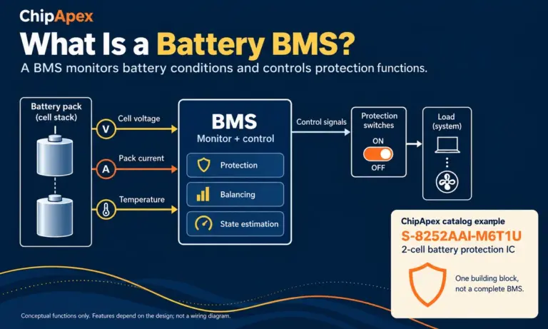
Learn what a battery BMS does, how protection differs from charging, and which pack specifications to check when sourcing BMS components through ChipApex.
Read More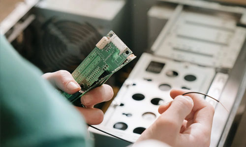
SN74AHCT125BQAR is listed in the Buffers, Drivers, Receivers, Transceivers range at ChipApex. The manufacturer field lists Texas Instruments. Its product description is 4-CH 4.5-V…
Read More
SN74AHCT125BQAR is listed in the Buffers, Drivers, Receivers, Transceivers range at ChipApex. The manufacturer field lists Texas Instruments. Its product description is 4-CH 4.5-V…
Read More
SN74AHCT125BQAR is listed in the Buffers, Drivers, Receivers, Transceivers range at ChipApex. The manufacturer field lists Texas Instruments. Its product description is 4-CH 4.5-V…
Read More
The activity of extra discounts on wholesale prices is in full swing…
Please fill in your contact information and we will send you the latest wholesale price list.





