 ChipApex | Global Electronic Components Supplier

SEARCH
Search Product
Search Post
— IC芯片 | 连接器 | 传感器 | 被动器件 —
Search productSearch post
— IC芯片 | 连接器 | 传感器 | 被动器件 —
Consult the customer manager about the wholesale price.
consultation hotline:86-132-6715-2157
email:[email protected]
Contact the product manager for consultation. One-stop consultation is available.
Do you want a lower wholesale price? Please send us your inquiry and we will reply immediately.
SN74ALVC16244ADL is listed in the Buffers, Drivers, Receivers, Transceivers range at ChipApex. The manufacturer field lists Texas Instruments. Its product description is IC BUF NON-INVERT 3.6V 48SSOP. Review the specifications below when checking this part for your BOM.
The SN74ALVC16244ADL is a 16-bit buffer and driver with 3-state outputs, manufactured by Texas Instruments. It operates from a supply voltage range of 1.65 V to 3.6 V and features a maximum propagation delay of 3 ns at 3.3 V. The device provides ±24 mA output drive capability at 3.3 V and includes latch-up performance exceeding 250 mA per JESD 17. It is housed in a 48-pin SSOP (DL) package and supports an operating free-air temperature range of -40 °C to 85 °C.
Verify that the specific ordering suffix matches the required package type, as the base model number corresponds to the SSOP variant. Confirm the moisture sensitivity level and lead finish details against the latest packaging addendum to ensure compatibility with assembly processes. Ensure all unused inputs are tied to VCC or GND to maintain proper operation.
Select this component when a 16-bit wide data path requires buffering with low propagation delay and strong drive current. It is suitable for applications needing operation across a wide voltage range from 1.65 V to 3.6 V. Consider the SSOP package constraints regarding pin count and thermal impedance if space is limited.
This device belongs to the Texas Instruments Widebus family, which focuses on improving performance and density for digital logic applications. It is part of the ALVC series, designed specifically for low-voltage CMOS operations. The ADL suffix indicates the SSOP package configuration, distinguishing it from other available form factors like TSSOP or FBGA.
SN74ALVC16244ADLR
All unused inputs must be held at VCC or GND to ensure proper device operation.
The OE input should be tied to VCC through a pullup resistor, with the minimum value determined by the driver's current-sinking capability.
Explore related parts through Logic, Integrated Circuits (ICs), all product categories, ChipApex homepage.
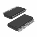 SN74ALVC16244ADL
SN74ALVC16244ADL is listed in the Buffers, Drivers, Receivers, Transceivers range at ChipApex. The manufacturer field lists Texas Instruments. Its product description is IC BUF…
Read More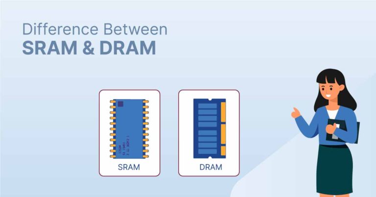
SN74ALVC16244ADL is listed in the Buffers, Drivers, Receivers, Transceivers range at ChipApex. The manufacturer field lists Texas Instruments. Its product description is IC BUF…
Read More
Choose an AC to DC converter by input range, output demand, isolation, efficiency and thermal derating. Compare architectures and check installation needs.
Read More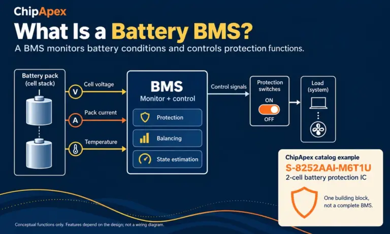
Learn what a battery BMS does, how protection differs from charging, and which pack specifications to check when sourcing BMS components through ChipApex.
Read More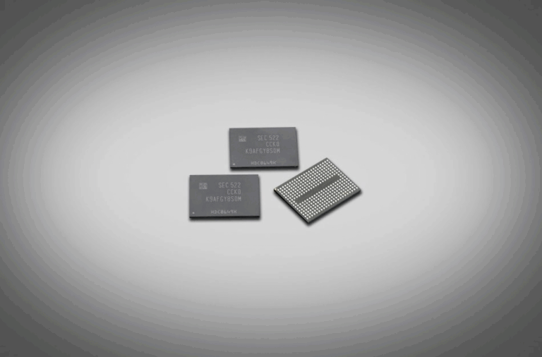
SN74ALVC16244ADL is listed in the Buffers, Drivers, Receivers, Transceivers range at ChipApex. The manufacturer field lists Texas Instruments. Its product description is IC BUF…
Read More
SN74ALVC16244ADL is listed in the Buffers, Drivers, Receivers, Transceivers range at ChipApex. The manufacturer field lists Texas Instruments. Its product description is IC BUF…
Read More
SN74ALVC16244ADL is listed in the Buffers, Drivers, Receivers, Transceivers range at ChipApex. The manufacturer field lists Texas Instruments. Its product description is IC BUF…
Read More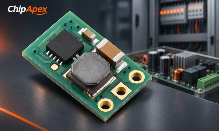
Select a DC-DC converter by input range, topology, isolation and temperature. Compare ripple, efficiency and load limits before choosing a component.
Read More
SN74ALVC16244ADL is listed in the Buffers, Drivers, Receivers, Transceivers range at ChipApex. The manufacturer field lists Texas Instruments. Its product description is IC BUF…
Read More
Find out when a bare shock switch needs a pull resistor, when an MCU internal pull-up is enough, and why sensor modules and piezo…
Read More
Learn what a shift register does, how bits move and when to use SIPO or PISO devices. Review latch timing, logic levels, output drive…
Read More
Learn the relay definition, coil and contact operation, NO and NC forms, load ratings and suppression choices. Compare mechanical, reed and solid-state types.
Read More
The activity of extra discounts on wholesale prices is in full swing…
Please fill in your contact information and we will send you the latest wholesale price list.





