 ChipApex | Global Electronic Components Supplier

SEARCH
Search Product
Search Post
— IC芯片 | 连接器 | 传感器 | 被动器件 —
Search productSearch post
— IC芯片 | 连接器 | 传感器 | 被动器件 —
Consult the customer manager about the wholesale price.
consultation hotline:86-132-6715-2157
email:[email protected]
Contact the product manager for consultation. One-stop consultation is available.
Do you want a lower wholesale price? Please send us your inquiry and we will reply immediately.
SN74ALVC244PW is listed in the Buffers, Drivers, Receivers, Transceivers range at ChipApex. The manufacturer field lists Texas Instruments. Its product description is IC BUF NON-INVERT 3.6V 20TSSOP. Review the specifications below when checking this part for your BOM.
The SN74ALVC244PW is an octal buffer and line driver with 3-state outputs manufactured by Texas Instruments. It operates from a supply voltage range of 1.65 V to 3.6 V. The device features two independent 4-bit drivers, each with a separate output-enable (OE) input. When OE is low, data passes from the A inputs to the Y outputs; when high, outputs enter a high-impedance state. Key electrical parameters include a maximum propagation delay of 2.8 ns at 3.3 V, ±24 mA output drive capability, and latch-up performance exceeding 250 mA per JESD 17. It is housed in a 20-pin TSSOP package.
Verify the specific ordering suffix against the manufacturer's current Package Option Addendum to confirm the exact packaging type, such as tube or tape-and-reel quantities. Ensure the moisture sensitivity level and peak reflow temperature ratings align with your assembly process requirements. Cross-reference the RoHS compliance status and lead finish specifications to guarantee compatibility with environmental regulations and soldering methods used in your manufacturing workflow.
Select this component when designing systems requiring low-power consumption and high-speed data transfer within a 1.65 V to 3.6 V supply range. The dual 4-bit configuration allows for independent control of output states, making it suitable for complex bus architectures. Consider the TSSOP-20 package dimensions if space constraints are critical, and ensure the ±24 mA drive strength meets the load requirements of the destination circuitry.
This device belongs to the ALVC logic family, designed for advanced low-voltage CMOS applications. It serves as a general-purpose buffer solution for digital systems transitioning from higher voltage standards to modern low-power environments. The octal configuration consolidates multiple buffer functions into a single compact integrated circuit, simplifying board layout and reducing component count in dense electronic designs.
SN74ALVC244PWR
When the OE input is low, the device passes data from the A inputs to the Y outputs. When OE is high, the outputs enter a high-impedance state, effectively disconnecting them from the bus.
To ensure the high-impedance state during power-up or power-down, the OE pin should be tied to VCC through a pullup resistor. The minimum resistor value is determined by the current-sinking capability of the driver.
Explore related parts through Logic, Integrated Circuits (ICs), all product categories, ChipApex homepage.
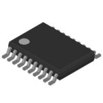 SN74ALVC244PW
SN74ALVC244PW is listed in the Buffers, Drivers, Receivers, Transceivers range at ChipApex. The manufacturer field lists Texas Instruments. Its product description is IC BUF…
Read More
Learn how rectifiers convert AC to DC, compare half-wave and bridge circuits, and select voltage, current, recovery and thermal ratings for your design.
Read More
SN74ALVC244PW is listed in the Buffers, Drivers, Receivers, Transceivers range at ChipApex. The manufacturer field lists Texas Instruments. Its product description is IC BUF…
Read More
SN74ALVC244PW is listed in the Buffers, Drivers, Receivers, Transceivers range at ChipApex. The manufacturer field lists Texas Instruments. Its product description is IC BUF…
Read More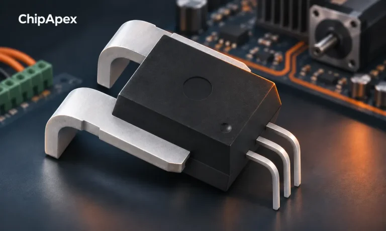
Compare Hall, shunt, current transformer and Rogowski sensing. Check AC/DC capability, accuracy, isolation, heat and response before selecting a sensor.
Read More
SN74ALVC244PW is listed in the Buffers, Drivers, Receivers, Transceivers range at ChipApex. The manufacturer field lists Texas Instruments. Its product description is IC BUF…
Read More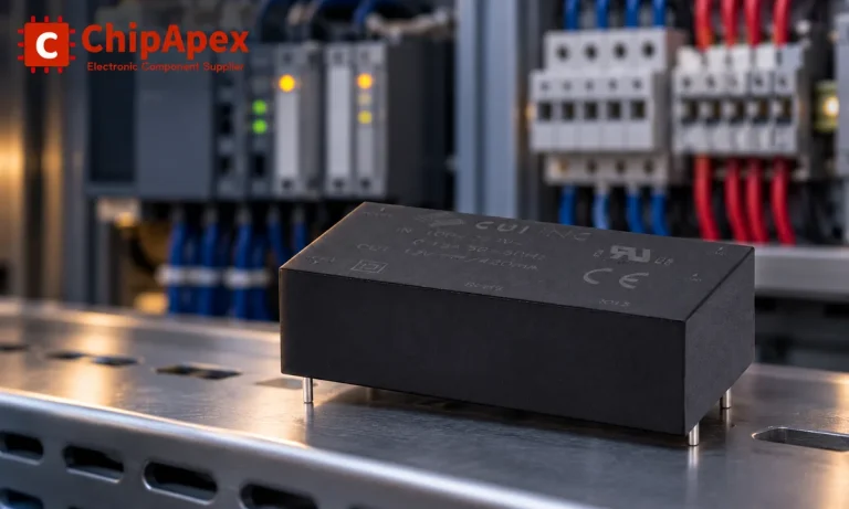
Choose an AC to DC converter by input range, output demand, isolation, efficiency and thermal derating. Compare architectures and check installation needs.
Read More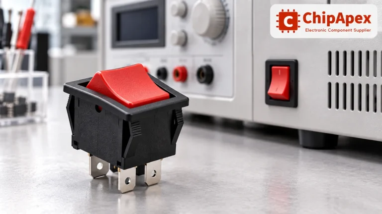
Choose a rocker switch by AC/DC ratings, contact arrangement, illumination, panel fit and sealing. Get practical checks for engineering and component sourcing.
Read MoreSN74ALVC244PW is listed in the Buffers, Drivers, Receivers, Transceivers range at ChipApex. The manufacturer field lists Texas Instruments. Its product description is IC BUF…
Read More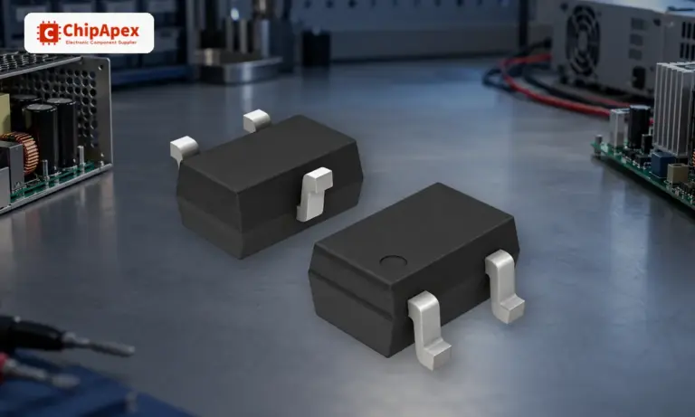
Learn how a diode conducts, how to identify anode and cathode, and when to choose rectifier, TVS, Zener or photodiode types for a circuit.
Read More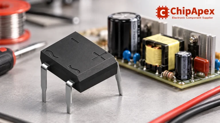
Select a bridge rectifier by reverse voltage, capacitor charging current, startup surge and cooling. Work through a stated DC voltage and ripple example.
Read More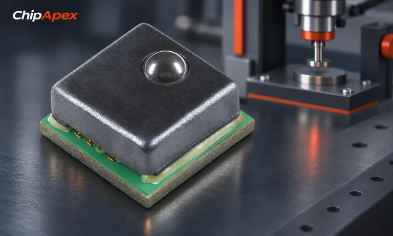
Understand load cell sensor output, bridge wiring and calibration. Learn how mV/V sensitivity, mechanics and ADC noise affect measurement accuracy.
Read More
The activity of extra discounts on wholesale prices is in full swing…
Please fill in your contact information and we will send you the latest wholesale price list.





