 ChipApex | Global Electronic Components Supplier

SEARCH
Search Product
Search Post
— IC芯片 | 连接器 | 传感器 | 被动器件 —
Search productSearch post
— IC芯片 | 连接器 | 传感器 | 被动器件 —
Consult the customer manager about the wholesale price.
consultation hotline:86-132-6715-2157
email:[email protected]
Contact the product manager for consultation. One-stop consultation is available.
Do you want a lower wholesale price? Please send us your inquiry and we will reply immediately.
SN74AUC1G07YEAR is listed in the Buffers, Drivers, Receivers, Transceivers range at ChipApex. The manufacturer field lists Texas Instruments. Its product description is IC BUFFER NON-INVERT 2.7V 5DSBGA. Review the specifications below when checking this part for your BOM.
The SN74AUC1G07YEAR is a single non-inverting buffer and line driver from the Texas Instruments AUC logic series. It operates within a supply voltage range of 0.8 V to 2.7 V, with specific design optimization for 1.65-V to 1.95-V applications. The device features an open-drain output capable of supporting active-low wired-OR or active-high wired-AND configurations. It provides ±8-mA output drive at 1.8 V and maintains low power consumption with a maximum ICC of 10 µA. Propagation delay is specified as a maximum of 2.5 ns at 1.8 V. The component utilizes the NanoStar YEA package, which employs die-as-package technology.
Verify the YEA suffix indicates the NanoStar WCSP package configuration. Confirm RoHS compliance status and moisture sensitivity level requirements for the specific manufacturing lot. Ensure the ordering part number matches the required tape and reel quantity specifications.
Select this component when open-drain output capability is required for wired-logic functions. The device is suitable for designs operating between 0.8 V and 2.7 V where sub-1-V operability is necessary. Consider the NanoStar package dimensions if board space constraints are critical.
This device belongs to the SN74AUC1G07 family of single buffers/drivers. It shares functional characteristics with other variants in the AUC Little Logic series but differs in physical packaging. The YEA suffix specifically denotes the NanoStar WCSP format with 0.17-mm small bumps.
SN74AUC1G07YEPR (NanoStar with large bumps)
The Ioff circuitry disables outputs to prevent damaging current backflow through the device during partial-power-down conditions.
The open-drain output allows connection to other open-drain outputs to implement active-low wired-OR or active-high wired-AND functions.
Explore related parts through Logic, Integrated Circuits (ICs), all product categories, ChipApex homepage.
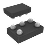 SN74AUC1G07YEAR
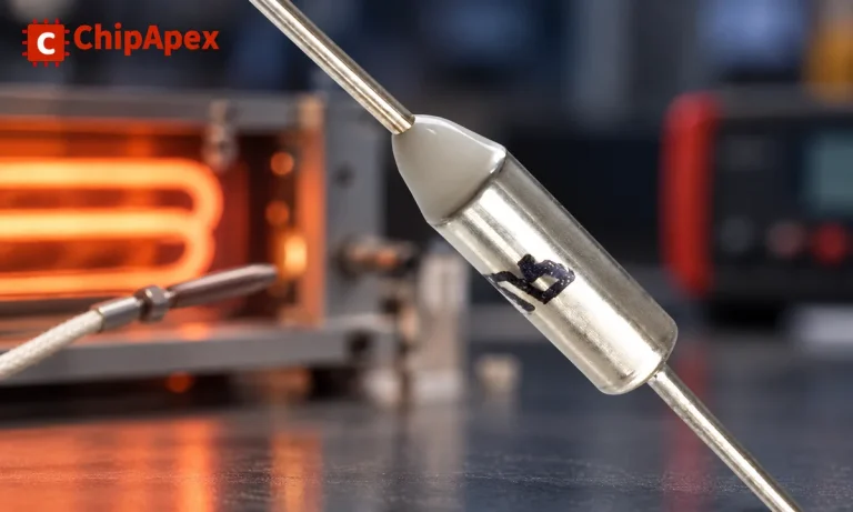
Understand thermal fuse operation, Tf, Th and Tm, electrical ratings and mounting. Check temperature limits and replacement requirements for your design.
Read More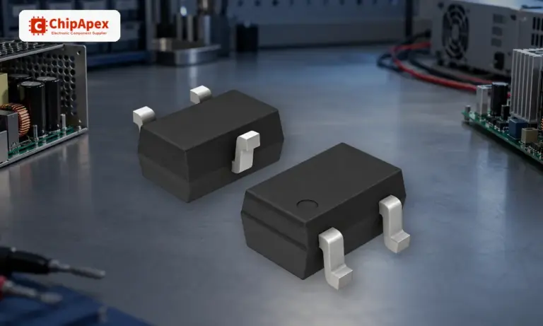
Learn how a diode conducts, how to identify anode and cathode, and when to choose rectifier, TVS, Zener or photodiode types for a circuit.
Read More
SN74AUC1G07YEAR is listed in the Buffers, Drivers, Receivers, Transceivers range at ChipApex. The manufacturer field lists Texas Instruments. Its product description is IC BUFFER…
Read More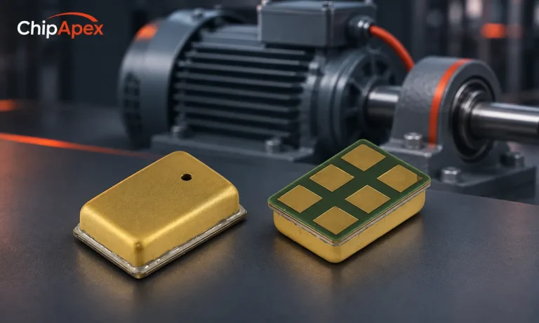
Choose a vibration sensor for machine monitoring. Compare sensing methods, bandwidth, noise and mounting, then define the signal-chain requirements.
Read More
SN74AUC1G07YEAR is listed in the Buffers, Drivers, Receivers, Transceivers range at ChipApex. The manufacturer field lists Texas Instruments. Its product description is IC BUFFER…
Read More
SN74AUC1G07YEAR is listed in the Buffers, Drivers, Receivers, Transceivers range at ChipApex. The manufacturer field lists Texas Instruments. Its product description is IC BUFFER…
Read More
SN74AUC1G07YEAR is listed in the Buffers, Drivers, Receivers, Transceivers range at ChipApex. The manufacturer field lists Texas Instruments. Its product description is IC BUFFER…
Read More
SN74AUC1G07YEAR is listed in the Buffers, Drivers, Receivers, Transceivers range at ChipApex. The manufacturer field lists Texas Instruments. Its product description is IC BUFFER…
Read More
SN74AUC1G07YEAR is listed in the Buffers, Drivers, Receivers, Transceivers range at ChipApex. The manufacturer field lists Texas Instruments. Its product description is IC BUFFER…
Read More
SN74AUC1G07YEAR is listed in the Buffers, Drivers, Receivers, Transceivers range at ChipApex. The manufacturer field lists Texas Instruments. Its product description is IC BUFFER…
Read More
Learn how an analog front end conditions sensor signals. Compare gain, noise, filtering, ADC settling and integration options before selecting components.
Read More
SN74AUC1G07YEAR is listed in the Buffers, Drivers, Receivers, Transceivers range at ChipApex. The manufacturer field lists Texas Instruments. Its product description is IC BUFFER…
Read More
The activity of extra discounts on wholesale prices is in full swing…
Please fill in your contact information and we will send you the latest wholesale price list.





