 ChipApex | Global Electronic Components Supplier

SEARCH
Search Product
Search Post
— IC芯片 | 连接器 | 传感器 | 被动器件 —
Search productSearch post
— IC芯片 | 连接器 | 传感器 | 被动器件 —
Consult the customer manager about the wholesale price.
consultation hotline:86-132-6715-2157
email:[email protected]
Contact the product manager for consultation. One-stop consultation is available.
Do you want a lower wholesale price? Please send us your inquiry and we will reply immediately.
SN74AUC1G125YEAR is listed in the Buffers, Drivers, Receivers, Transceivers range at ChipApex. The manufacturer field lists Texas Instruments. Its product description is IC BUFFER NON-INVERT 2.7V 5DSBGA. Review the specifications below when checking this part for your BOM.
The SN74AUC1G125 is a single bus buffer gate with 3-state output from the Texas Instruments AUC logic family. It operates within a supply voltage range of 0.8 V to 2.7 V and is optimized for 1.65-V to 1.95-V operation. The device features over-voltage tolerant I/Os supporting up to 3.6 V independent of VCC, an Ioff feature for partial power down mode, and low power consumption with a maximum ICC of 10 µA. Latch-up performance exceeds 100 mA per JESD 78, Class II.
Verify the specific package suffix (DBV, DCK, or YZP) matches the required footprint. Confirm RoHS compliance and lead finish details in the orderable addendum. Ensure design accounts for active-low OE functionality and proper termination of unused inputs to prevent floating states.
Select this component for applications requiring ultra-low voltage operation and high speed. The AUC family provides excellent signal integrity for driving controlled impedance transmission lines without external termination. Consider thermal resistance values when designing for dense PCB layouts.
This device belongs to the SN74AUC1G series, designed for speed and optimized for sub-1-V little logic operations. It utilizes ULTTL outputs for balanced sourcing and sinking capabilities, ensuring minimal switching noise while maintaining optimal signal integrity across the specified voltage range.
SN74AUC1G125DBVR
The Ioff circuitry disables all outputs when the supply pin is held at 0 V, preventing damaging current backflow through the device during partial power-down conditions.
All unused inputs must be connected to a logic high or logic low voltage (VCC or GND) to prevent undefined operational states and excessive power consumption caused by floating inputs.
Explore related parts through Logic, Integrated Circuits (ICs), all product categories, ChipApex homepage.
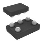 SN74AUC1G125YEAR
Learn how rectifiers convert AC to DC, compare half-wave and bridge circuits, and select voltage, current, recovery and thermal ratings for your design.
Read More
SN74AUC1G125YEAR is listed in the Buffers, Drivers, Receivers, Transceivers range at ChipApex. The manufacturer field lists Texas Instruments. Its product description is IC BUFFER…
Read More
SN74AUC1G125YEAR is listed in the Buffers, Drivers, Receivers, Transceivers range at ChipApex. The manufacturer field lists Texas Instruments. Its product description is IC BUFFER…
Read More
Understand load cell sensor output, bridge wiring and calibration. Learn how mV/V sensitivity, mechanics and ADC noise affect measurement accuracy.
Read More
Understand RF attenuator dB values, fixed and programmable types, impedance, power limits and noise tradeoffs before choosing parts for an RF signal path.
Read More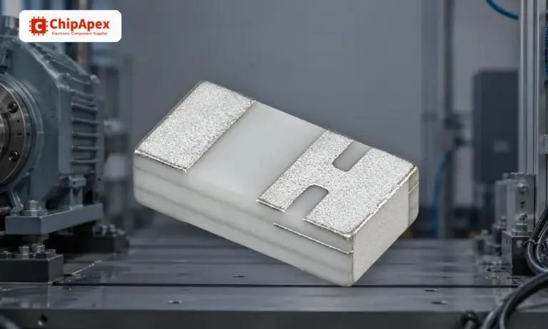
Find out when a bare shock switch needs a pull resistor, when an MCU internal pull-up is enough, and why sensor modules and piezo…
Read More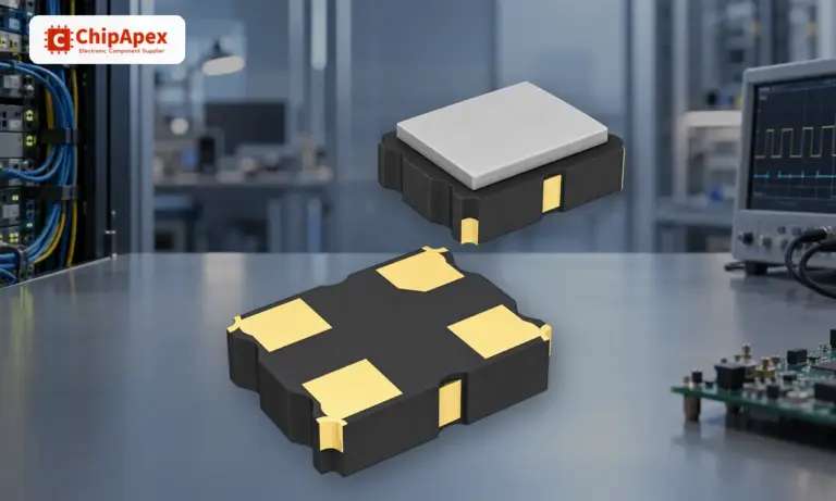
Understand how oscillators generate timing signals, how they differ from crystals, and which frequency, output and stability specs matter when choosing one.
Read More
SN74AUC1G125YEAR is listed in the Buffers, Drivers, Receivers, Transceivers range at ChipApex. The manufacturer field lists Texas Instruments. Its product description is IC BUFFER…
Read More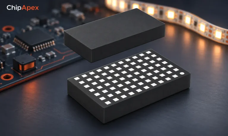
Choose LED drivers by current, string voltage, dimming and thermal limits. Understand constant-current operation and the checks needed for your load.
Read More
SN74AUC1G125YEAR is listed in the Buffers, Drivers, Receivers, Transceivers range at ChipApex. The manufacturer field lists Texas Instruments. Its product description is IC BUFFER…
Read More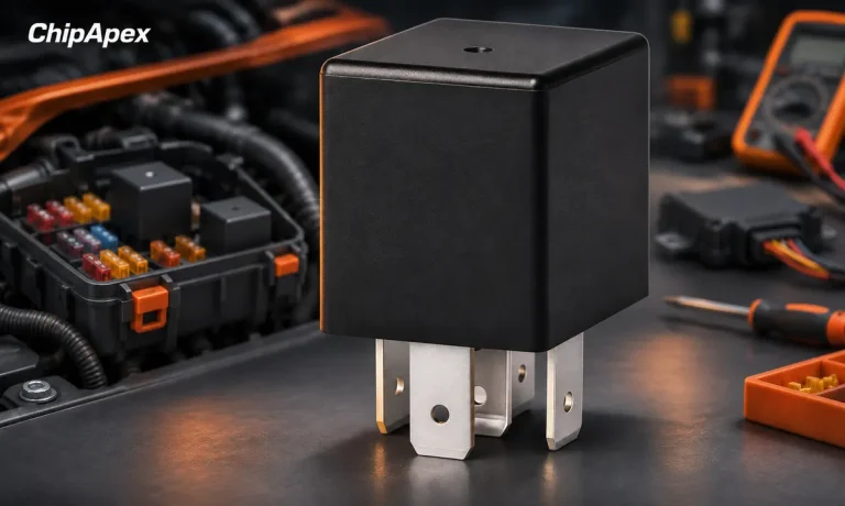
Understand automotive relay terminals, coil suppression and load ratings. Check inrush, socket compatibility and temperature before selecting a replacement.
Read More
SN74AUC1G125YEAR is listed in the Buffers, Drivers, Receivers, Transceivers range at ChipApex. The manufacturer field lists Texas Instruments. Its product description is IC BUFFER…
Read More
The activity of extra discounts on wholesale prices is in full swing…
Please fill in your contact information and we will send you the latest wholesale price list.





