 ChipApex | Global Electronic Components Supplier

SEARCH
Search Product
Search Post
— IC芯片 | 连接器 | 传感器 | 被动器件 —
Search productSearch post
— IC芯片 | 连接器 | 传感器 | 被动器件 —
Consult the customer manager about the wholesale price.
consultation hotline:86-132-6715-2157
email:[email protected]
Contact the product manager for consultation. One-stop consultation is available.
Do you want a lower wholesale price? Please send us your inquiry and we will reply immediately.
SN74BCT244NS is listed in the Buffers, Drivers, Receivers, Transceivers range at ChipApex. The manufacturer field lists Texas Instruments. Its product description is PROTOTYPE. Review the specifications below when checking this part for your BOM.
The SN74BCT244NS is an octal buffer and line driver utilizing BiCMOS technology. It features two independent 4-bit buffers with separate active-low output-enable (OE) inputs. The device provides non-inverting data transfer from A inputs to Y outputs when OE is low, entering a high-impedance state when OE is high. It operates within a supply voltage range of 4.5 V to 5.5 V. Electrical characteristics include a maximum low-level output current of 64 mA and a typical propagation delay of 3.2 ns at 5 V with a 50 pF load.
Verify the specific ordering suffix 'NS' corresponds to the SOP package configuration before procurement. Confirm that the required operating temperature range aligns with the commercial specification of 0°C to 70°C. Ensure compatibility with the 4.5 V to 5.5 V supply voltage requirements for the target application environment.
Select this component for applications requiring high drive strength and reduced power consumption compared to standard TTL logic. The BiCMOS architecture offers superior performance for bus driving tasks. Consider the SOP package dimensions for PCB layout constraints. Verify that the input voltage levels are compatible with the source logic family.
This device belongs to the Texas Instruments BCT logic family, which combines CMOS density with Bipolar drive strength. It complements the inverting BCT240 and BCT241 variants, allowing designers to mix polarities within a system. The SN74BCT244 specifically provides non-inverting functionality for signal buffering and isolation purposes.
SN74BCT244N
The OE (Output Enable) pin controls the output state. When OE is low, data passes from inputs to outputs. When OE is high, the outputs enter a high-impedance state.
The device is organized as two independent 4-bit buffers/line drivers, each with its own separate output-enable input.
Explore related parts through Logic, Integrated Circuits (ICs), all product categories, ChipApex homepage.
 SN74BCT244NS

SN74BCT244NS is listed in the Buffers, Drivers, Receivers, Transceivers range at ChipApex. The manufacturer field lists Texas Instruments. Its product description is PROTOTYPE. Review…
Read More
SN74BCT244NS is listed in the Buffers, Drivers, Receivers, Transceivers range at ChipApex. The manufacturer field lists Texas Instruments. Its product description is PROTOTYPE. Review…
Read More
Understand how a comparator switches at a voltage threshold, why hysteresis prevents chatter, and which output and input specs matter.
Read More
SN74BCT244NS is listed in the Buffers, Drivers, Receivers, Transceivers range at ChipApex. The manufacturer field lists Texas Instruments. Its product description is PROTOTYPE. Review…
Read More
SN74BCT244NS is listed in the Buffers, Drivers, Receivers, Transceivers range at ChipApex. The manufacturer field lists Texas Instruments. Its product description is PROTOTYPE. Review…
Read More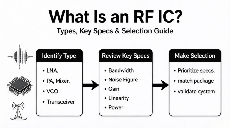
SN74BCT244NS is listed in the Buffers, Drivers, Receivers, Transceivers range at ChipApex. The manufacturer field lists Texas Instruments. Its product description is PROTOTYPE. Review…
Read More
SN74BCT244NS is listed in the Buffers, Drivers, Receivers, Transceivers range at ChipApex. The manufacturer field lists Texas Instruments. Its product description is PROTOTYPE. Review…
Read More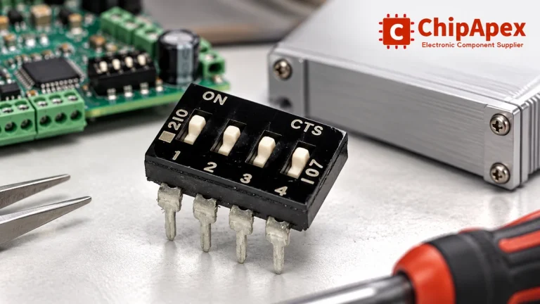
Choose a DIP switch by contact type, coded positions, footprint and signal ratings. Check logic polarity, assembly conditions and PCB configuration behavior.
Read More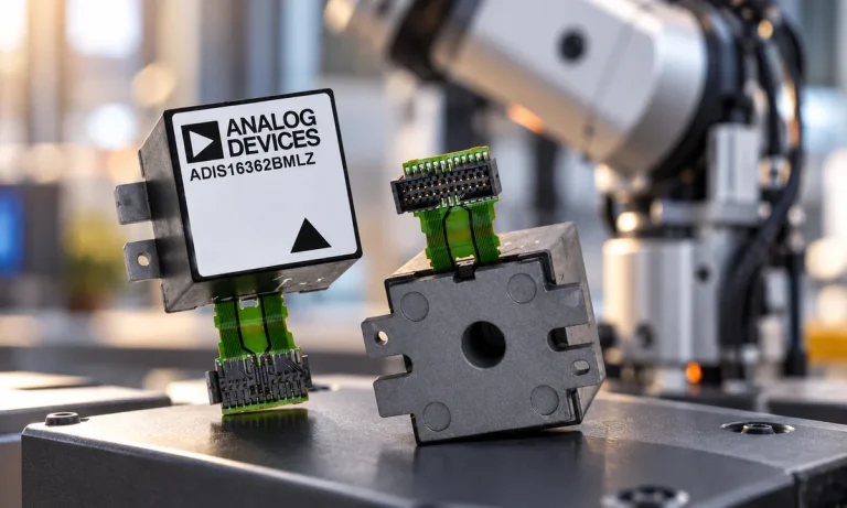
Learn what an IMU measures, how accelerometers and gyroscopes work together, why orientation estimates drift, and what to compare.
Read More
SN74BCT244NS is listed in the Buffers, Drivers, Receivers, Transceivers range at ChipApex. The manufacturer field lists Texas Instruments. Its product description is PROTOTYPE. Review…
Read More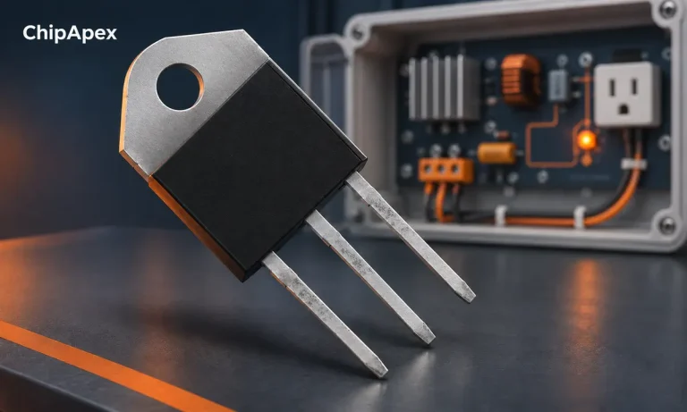
Learn how a TRIAC switches AC loads. Understand triggering, latching, holding current, phase control and thermal limits before choosing a component.
Read More
Learn what a shift register does, how bits move and when to use SIPO or PISO devices. Review latch timing, logic levels, output drive…
Read More
The activity of extra discounts on wholesale prices is in full swing…
Please fill in your contact information and we will send you the latest wholesale price list.





