 ChipApex | Global Electronic Components Supplier

SEARCH
Search Product
Search Post
— IC芯片 | 连接器 | 传感器 | 被动器件 —
Search productSearch post
— IC芯片 | 连接器 | 传感器 | 被动器件 —
Consult the customer manager about the wholesale price.
consultation hotline:86-132-6715-2157
email:[email protected]
Contact the product manager for consultation. One-stop consultation is available.
Do you want a lower wholesale price? Please send us your inquiry and we will reply immediately.
SN74BCT541ANS is listed in the Buffers, Drivers, Receivers, Transceivers range at ChipApex. The manufacturer field lists Texas Instruments. Its product description is PROTOTYPE. Review the specifications below when checking this part for your BOM.
The SN74BCT541ANS is an octal buffer and line driver manufactured by Texas Instruments, utilizing state-of-the-art BiCMOS technology. It features non-inverting logic with 3-state outputs controlled by two active-low output-enable inputs (OE1 and OE2). The device operates within a supply voltage range of 4.5 V to 5.5 V and supports an operating temperature range of 0°C to 70°C. Packaged in a 20-pin Small Outline Package (NS), it provides high drive capability with low power consumption characteristics typical of the BCT family.
Verify the specific ordering suffix 'ANS' corresponds to the SOP-20 package configuration. Confirm RoHS compliance status and lead finish details via the manufacturer's official documentation. Ensure the application environment remains within the specified 0°C to 70°C operating temperature range for reliable performance.
Select this component for applications requiring octal buffering with high-speed performance and low power dissipation. The BiCMOS technology offers a balance between speed and static power consumption. Verify that the required operating temperature range aligns with the commercial grade specifications of the SN74BCT541A series.
This part belongs to the SN54/74BCT541 family of octal buffers/drivers with 3-state outputs. The BCT series combines BiCMOS technology with TTL-compatible input levels, offering faster switching speeds than standard CMOS while maintaining lower power consumption than bipolar families. The 'A' designation indicates the specific revision of the SN74BCT541 device.
SN74BCT541ADW
The outputs are controlled by two active-low output-enable inputs (OE1 and OE2). If either input is high, all eight outputs enter a high-impedance state.
To ensure the high-impedance state during power-up or power-down, the OE inputs should be tied to VCC through a pullup resistor.
Explore related parts through Logic, Integrated Circuits (ICs), all product categories, ChipApex homepage.
 SN74BCT541ANS
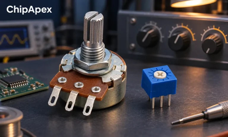
Compare rheostat and potentiometer wiring and functions. Understand divider loading, wiper current, track power and practical component selection.
Read More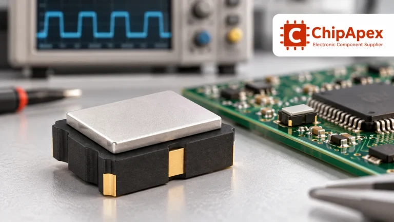
Compare RC, crystal and MEMS oscillator circuits. Check ppm, jitter, load capacitance, startup margin and output compatibility before choosing a clock source.
Read More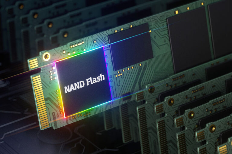
SN74BCT541ANS is listed in the Buffers, Drivers, Receivers, Transceivers range at ChipApex. The manufacturer field lists Texas Instruments. Its product description is PROTOTYPE. Review…
Read More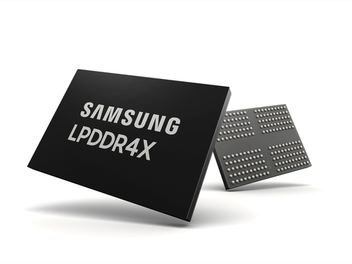
SN74BCT541ANS is listed in the Buffers, Drivers, Receivers, Transceivers range at ChipApex. The manufacturer field lists Texas Instruments. Its product description is PROTOTYPE. Review…
Read More
SN74BCT541ANS is listed in the Buffers, Drivers, Receivers, Transceivers range at ChipApex. The manufacturer field lists Texas Instruments. Its product description is PROTOTYPE. Review…
Read More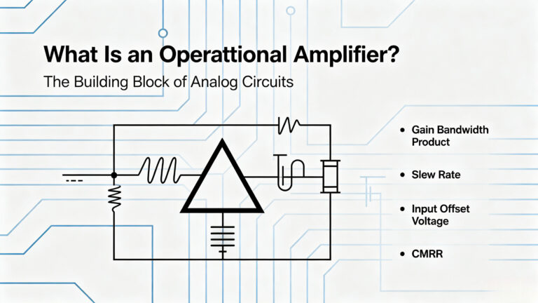
SN74BCT541ANS is listed in the Buffers, Drivers, Receivers, Transceivers range at ChipApex. The manufacturer field lists Texas Instruments. Its product description is PROTOTYPE. Review…
Read More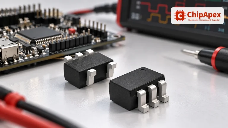
Choose logic inverter ICs by thresholds, supply, output drive and delay. Compare standard and Schmitt-trigger inputs, power sequencing and replacement checks.
Read More
SN74BCT541ANS is listed in the Buffers, Drivers, Receivers, Transceivers range at ChipApex. The manufacturer field lists Texas Instruments. Its product description is PROTOTYPE. Review…
Read More
SN74BCT541ANS is listed in the Buffers, Drivers, Receivers, Transceivers range at ChipApex. The manufacturer field lists Texas Instruments. Its product description is PROTOTYPE. Review…
Read More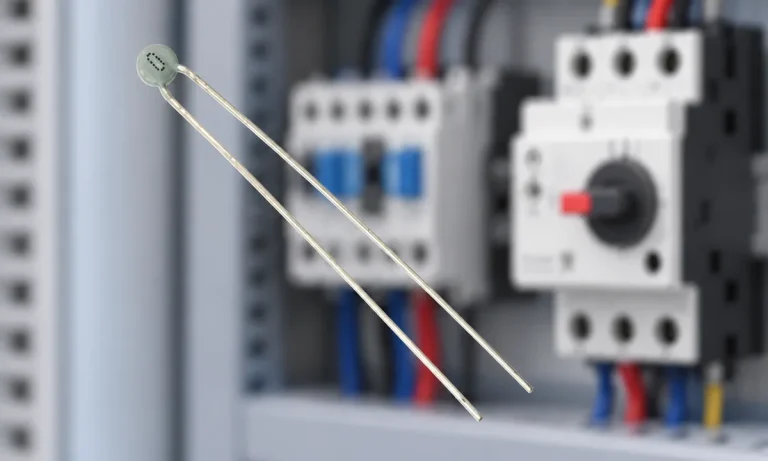
Learn why PTC resistance rises with temperature, how it differs from NTC, and which ratings matter for sensing and protection.
Read More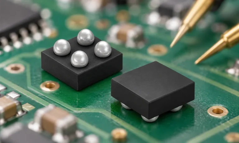
Understand how a comparator switches at a voltage threshold, why hysteresis prevents chatter, and which output and input specs matter.
Read More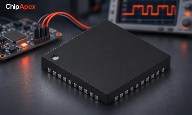
Understand UART protocol framing, baud rate and electrical interfaces. Learn 8N1 timing, TX/RX wiring, buffering and practical troubleshooting steps.
Read More
The activity of extra discounts on wholesale prices is in full swing…
Please fill in your contact information and we will send you the latest wholesale price list.





