 ChipApex | Global Electronic Components Supplier

SEARCH
Search Product
Search Post
— IC芯片 | 连接器 | 传感器 | 被动器件 —
Search productSearch post
— IC芯片 | 连接器 | 传感器 | 被动器件 —
Consult the customer manager about the wholesale price.
consultation hotline:86-132-6715-2157
email:[email protected]
Contact the product manager for consultation. One-stop consultation is available.
Do you want a lower wholesale price? Please send us your inquiry and we will reply immediately.
SN74HC365PWTE4 is listed in the Buffers, Drivers, Receivers, Transceivers range at ChipApex. The manufacturer field lists Texas Instruments. Its product description is IC BUFFER NON-INVERT 6V 16TSSOP. Review the specifications below when checking this part for your BOM.
The SN74HC365PWTE4 is a hex buffer and line driver with 3-state outputs manufactured by Texas Instruments. It operates within a supply voltage range of 2 V to 6 V and supports an operating temperature range of -40°C to +85°C. The device features six independent non-inverting buffers with dual-gated output-enable inputs (OE1 and OE2). Propagation delay is typically 10 ns, with maximum values reaching 120 ns at 2 V and 20 ns at 6 V. Output drive capability includes ±6 mA at 5 V.
Verify the specific package type and tape-and-reel configuration against the orderable addendum in the datasheet. Confirm RoHS compliance and lead finish details as these may vary across production revisions. Ensure the component status matches current availability requirements before finalizing procurement plans.
Select this component for designs requiring multiple buffered signals with controlled tri-state behavior on a shared bus. The HC logic family offers low power consumption suitable for battery-operated systems. Verify input transition rise/fall time limits to ensure signal integrity within the specified operating conditions.
This part belongs to the SNx4HC365 series of hex buffers and line drivers. It is designed to improve performance and density in digital circuits compared to standard logic families. The device provides true outputs and is available in various packages including TSSOP, SOIC, and PDIP.
SN74HC365PWR
All channels enter the high-impedance state when either of the output enable (OE) pins is set to the high state. Data passes from A inputs to Y outputs only when both OE1 and OE2 are low.
A 0.1-μF capacitor is recommended for each VCC terminal to prevent power disturbance. It should be installed as close to the power terminal as possible.
Explore related parts through Logic, Integrated Circuits (ICs), all product categories, ChipApex homepage.
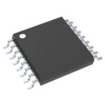 SN74HC365PWTE4
SN74HC365PWTE4 is listed in the Buffers, Drivers, Receivers, Transceivers range at ChipApex. The manufacturer field lists Texas Instruments. Its product description is IC BUFFER…
Read More
SN74HC365PWTE4 is listed in the Buffers, Drivers, Receivers, Transceivers range at ChipApex. The manufacturer field lists Texas Instruments. Its product description is IC BUFFER…
Read More
Understand how a comparator switches at a voltage threshold, why hysteresis prevents chatter, and which output and input specs matter.
Read More
SN74HC365PWTE4 is listed in the Buffers, Drivers, Receivers, Transceivers range at ChipApex. The manufacturer field lists Texas Instruments. Its product description is IC BUFFER…
Read More
SN74HC365PWTE4 is listed in the Buffers, Drivers, Receivers, Transceivers range at ChipApex. The manufacturer field lists Texas Instruments. Its product description is IC BUFFER…
Read More
SN74HC365PWTE4 is listed in the Buffers, Drivers, Receivers, Transceivers range at ChipApex. The manufacturer field lists Texas Instruments. Its product description is IC BUFFER…
Read More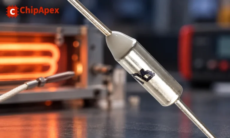
Understand thermal fuse operation, Tf, Th and Tm, electrical ratings and mounting. Check temperature limits and replacement requirements for your design.
Read More
Select a bridge rectifier by reverse voltage, capacitor charging current, startup surge and cooling. Work through a stated DC voltage and ripple example.
Read More
Compare RC, crystal and MEMS oscillator circuits. Check ppm, jitter, load capacitance, startup margin and output compatibility before choosing a clock source.
Read More
SN74HC365PWTE4 is listed in the Buffers, Drivers, Receivers, Transceivers range at ChipApex. The manufacturer field lists Texas Instruments. Its product description is IC BUFFER…
Read More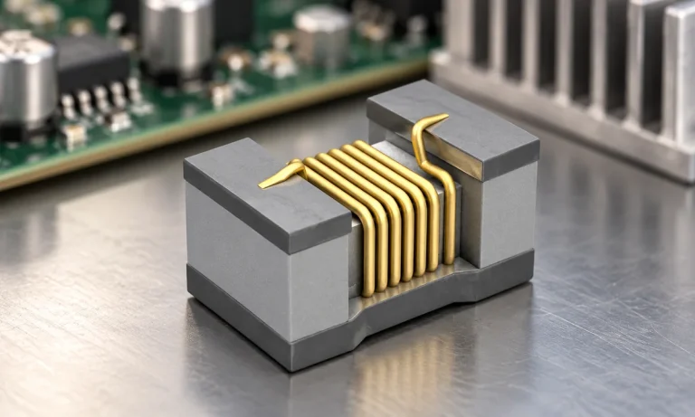
See when an inductor behaves linearly, how DC bias and saturation reduce inductance, and which current and temperature curves to check.
Read More
Compare thermistors, RTDs, thermocouples and temperature ICs. Learn how range, accuracy, response, interfaces and mounting affect component selection.
Read More
The activity of extra discounts on wholesale prices is in full swing…
Please fill in your contact information and we will send you the latest wholesale price list.





