 ChipApex | Global Electronic Components Supplier

SEARCH
Search Product
Search Post
— IC芯片 | 连接器 | 传感器 | 被动器件 —
Search productSearch post
— IC芯片 | 连接器 | 传感器 | 被动器件 —
Consult the customer manager about the wholesale price.
consultation hotline:86-132-6715-2157
email:[email protected]
Contact the product manager for consultation. One-stop consultation is available.
Do you want a lower wholesale price? Please send us your inquiry and we will reply immediately.
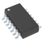
SN74HCS08QDYYRQ1 is listed in the Inverter Gates range at ChipApex. The manufacturer field lists Texas Instruments. Its product description is IC GATE AND 4CH 2-INP 14SOT23. Review the specifications below when checking this part for your BOM.
The SN74HCS08QDYYRQ1 is an automotive-grade quadruple 2-input AND gate featuring Schmitt-trigger inputs. It operates within a supply voltage range of 2 V to 6 V and supports ambient temperatures from -40°C to +125°C. The device provides balanced CMOS push-pull outputs with ±7.8 mA drive capability at 6 V. Propagation delay ranges from 6 ns to 36 ns depending on voltage. It includes HBM ESD Level 2 and CDM Level C6 ratings, with typical supply current of 100 nA.
Verify the specific DYY package designation (SOT-23-THIN) matches the target PCB footprint requirements. Confirm that the AEC-Q100 qualification aligns with the specific automotive grade requirements of the end application. Ensure design margins account for the specified thermal resistance values associated with this small outline package type.
Select this component when noisy environments require Schmitt-trigger hysteresis to prevent false triggering. Choose this part for designs needing wide voltage flexibility between 2 V and 6 V. Consider the SOT-23-THIN package constraints regarding thermal dissipation and board space limitations compared to larger SOIC or TSSOP alternatives.
This device belongs to the SN74HCS08-Q1 family of automotive logic gates. It shares functional characteristics with other members like SN74HCS08PW-Q1 and SN74HCS08D-Q1, differing primarily in physical packaging dimensions and thermal properties. The Q1 suffix indicates automotive reliability compliance.
SN74HCS08PW-Q1
It allows the device to tolerate slow or noisy input signals without causing undefined states or excessive dynamic current consumption.
Unused inputs must not be left floating; they should be terminated to either VCC or ground to ensure defined operational states.
Explore related parts through Logic, Integrated Circuits (ICs), all product categories, ChipApex homepage.
 SN74HCS08QDYYRQ1
SN74HCS08QDYYRQ1 is listed in the Inverter Gates range at ChipApex. The manufacturer field lists Texas Instruments. Its product description is IC GATE AND 4CH…
Read More
SN74HCS08QDYYRQ1 is listed in the Inverter Gates range at ChipApex. The manufacturer field lists Texas Instruments. Its product description is IC GATE AND 4CH…
Read More
SN74HCS08QDYYRQ1 is listed in the Inverter Gates range at ChipApex. The manufacturer field lists Texas Instruments. Its product description is IC GATE AND 4CH…
Read More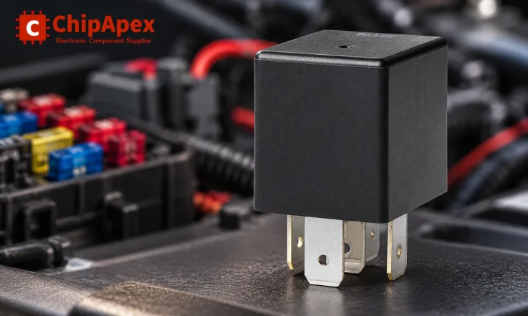
Learn the relay definition, coil and contact operation, NO and NC forms, load ratings and suppression choices. Compare mechanical, reed and solid-state types.
Read More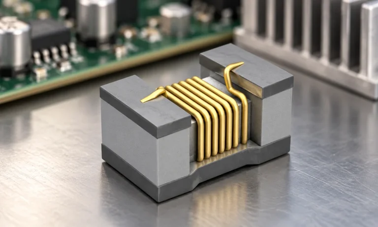
See when an inductor behaves linearly, how DC bias and saturation reduce inductance, and which current and temperature curves to check.
Read More
SN74HCS08QDYYRQ1 is listed in the Inverter Gates range at ChipApex. The manufacturer field lists Texas Instruments. Its product description is IC GATE AND 4CH…
Read More
SN74HCS08QDYYRQ1 is listed in the Inverter Gates range at ChipApex. The manufacturer field lists Texas Instruments. Its product description is IC GATE AND 4CH…
Read More
SN74HCS08QDYYRQ1 is listed in the Inverter Gates range at ChipApex. The manufacturer field lists Texas Instruments. Its product description is IC GATE AND 4CH…
Read More
SN74HCS08QDYYRQ1 is listed in the Inverter Gates range at ChipApex. The manufacturer field lists Texas Instruments. Its product description is IC GATE AND 4CH…
Read More
SN74HCS08QDYYRQ1 is listed in the Inverter Gates range at ChipApex. The manufacturer field lists Texas Instruments. Its product description is IC GATE AND 4CH…
Read More
SN74HCS08QDYYRQ1 is listed in the Inverter Gates range at ChipApex. The manufacturer field lists Texas Instruments. Its product description is IC GATE AND 4CH…
Read MoreSN74HCS08QDYYRQ1 is listed in the Inverter Gates range at ChipApex. The manufacturer field lists Texas Instruments. Its product description is IC GATE AND 4CH…
Read More
The activity of extra discounts on wholesale prices is in full swing…
Please fill in your contact information and we will send you the latest wholesale price list.





