 ChipApex | Global Electronic Components Supplier

SEARCH
Search Product
Search Post
— IC芯片 | 连接器 | 传感器 | 被动器件 —
Search productSearch post
— IC芯片 | 连接器 | 传感器 | 被动器件 —
Consult the customer manager about the wholesale price.
consultation hotline:86-132-6715-2157
email:[email protected]
Contact the product manager for consultation. One-stop consultation is available.
Do you want a lower wholesale price? Please send us your inquiry and we will reply immediately.
SN74HCS367DR is listed in the Buffers, Drivers, Receivers, Transceivers range at ChipApex. The manufacturer field lists Texas Instruments. Its product description is IC BUFFER NON-INVERT 6V 16SOIC. Review the specifications below when checking this part for your BOM.
The SN74HCS367DR is a hex buffer and line driver manufactured by Texas Instruments, featuring Schmitt-trigger inputs and three-state outputs. It operates within a supply voltage range of 2 V to 6 V and supports an extended ambient temperature range from -40°C to +125°C. The device provides balanced CMOS outputs capable of sourcing and sinking up to 7.8 mA at 6 V. It consumes low power with a typical supply current of 100 nA. The component is housed in a 16-pin SOIC package.
Verify the specific ordering suffix 'DR' corresponds to the SOIC-16 surface-mount package configuration. Confirm that the required operating temperature range aligns with the specified -40°C to +125°C limits. Ensure input signals remain within the absolute maximum ratings to prevent damage from overvoltage or excessive clamp currents. Validate that the load capacitance does not exceed recommended levels for optimal switching performance.
Select this component when noise immunity is critical due to its Schmitt-trigger architecture. It is suitable for applications requiring signal buffering with controlled output states. Consider the 2 V to 6 V supply range compatibility with the system logic levels. Evaluate the thermal resistance characteristics if operating near the upper temperature limit. Ensure the drive current requirements do not exceed the 7.8 mA capability per output.
This device belongs to the SN74HCS series of high-speed CMOS logic components. It shares functional similarities with other hex buffers but distinguishes itself through integrated Schmitt-trigger inputs. The three-state output capability allows for bus sharing and signal gating. It serves as a robust interface solution between controllers and peripheral devices in complex digital systems.
SN74HC367DR
Unused inputs must be terminated to either VCC or ground to prevent undefined operational states caused by floating voltages.
The output enable (OE) pins control the state of each bank of buffers. A low state enables the outputs, while a high state places them in a high-impedance state.
Explore related parts through Logic, Integrated Circuits (ICs), all product categories, ChipApex homepage.
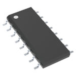 SN74HCS367DR

SN74HCS367DR is listed in the Buffers, Drivers, Receivers, Transceivers range at ChipApex. The manufacturer field lists Texas Instruments. Its product description is IC BUFFER…
Read More
Explore electronic component types, functions, packages and datasheets. Learn selection, replacement and BOM checks before ordering parts for your PCB.
Read More
Choose a pin header by pitch, mating geometry, current rating and mounting. Learn why matching pin count and spacing does not guarantee compatibility.
Read More
Understand how oscillators generate timing signals, how they differ from crystals, and which frequency, output and stability specs matter when choosing one.
Read More
Understand how a comparator switches at a voltage threshold, why hysteresis prevents chatter, and which output and input specs matter.
Read More
SN74HCS367DR is listed in the Buffers, Drivers, Receivers, Transceivers range at ChipApex. The manufacturer field lists Texas Instruments. Its product description is IC BUFFER…
Read More
Compare gas sensor technologies, cross-sensitivity and calibration needs. Define the gas, range and environment before choosing a sensing component.
Read More
Choose a DIP switch by contact type, coded positions, footprint and signal ratings. Check logic polarity, assembly conditions and PCB configuration behavior.
Read More
SN74HCS367DR is listed in the Buffers, Drivers, Receivers, Transceivers range at ChipApex. The manufacturer field lists Texas Instruments. Its product description is IC BUFFER…
Read MoreSN74HCS367DR is listed in the Buffers, Drivers, Receivers, Transceivers range at ChipApex. The manufacturer field lists Texas Instruments. Its product description is IC BUFFER…
Read More
SN74HCS367DR is listed in the Buffers, Drivers, Receivers, Transceivers range at ChipApex. The manufacturer field lists Texas Instruments. Its product description is IC BUFFER…
Read More
SN74HCS367DR is listed in the Buffers, Drivers, Receivers, Transceivers range at ChipApex. The manufacturer field lists Texas Instruments. Its product description is IC BUFFER…
Read More
The activity of extra discounts on wholesale prices is in full swing…
Please fill in your contact information and we will send you the latest wholesale price list.





