 ChipApex | Global Electronic Components Supplier

SEARCH
Search Product
Search Post
— IC芯片 | 连接器 | 传感器 | 被动器件 —
Search productSearch post
— IC芯片 | 连接器 | 传感器 | 被动器件 —
Consult the customer manager about the wholesale price.
consultation hotline:86-132-6715-2157
email:[email protected]
Contact the product manager for consultation. One-stop consultation is available.
Do you want a lower wholesale price? Please send us your inquiry and we will reply immediately.
SN74HCS367PWR is listed in the Buffers, Drivers, Receivers, Transceivers range at ChipApex. The manufacturer field lists Texas Instruments. Its product description is IC BUFFER NON-INVERT 6V 16TSSOP. Review the specifications below when checking this part for your BOM.
The SN74HCS367PWR is a hex buffer and line driver featuring Schmitt-trigger inputs and three-state outputs, manufactured by Texas Instruments. It operates within a supply voltage range of 2 V to 6 V and supports an extended ambient temperature range from -40°C to +125°C. The device provides balanced CMOS outputs capable of sourcing and sinking up to 7.8 mA at 6 V. It includes low power consumption characteristics with typical supply current of 100 nA. The component is housed in a TSSOP-16 package.
Verify the specific ordering suffix 'PW' corresponds to the TSSOP-16 package variant when procuring. Confirm that the required operating temperature range aligns with the specified -40°C to +125°C limits. Ensure supply voltage constraints between 2 V and 6 V are met for proper functionality. Check for any recent documentation updates regarding pin configurations or electrical characteristics before finalizing design integration.
Select this component when noise immunity is critical due to its Schmitt-trigger architecture. It is suitable for applications requiring signal buffering with controlled output states. Consider the TSSOP-16 package size if space constraints exist on the PCB. Verify that the load capacitance does not exceed recommended limits to maintain switching performance specifications.
This device belongs to the SN74HCS series of high-speed CMOS logic devices. It functions as a hex buffer with distinct banks controlled by separate output enable pins. The HCS designation indicates the inclusion of Schmitt-trigger inputs, differentiating it from standard HC series components which lack hysteresis features.
SN74HCS367D (SOIC-16 package)
The device is configured into two banks: one containing four drivers and another containing two drivers, each controlled by its own active-low output enable pin.
When the output enable pin is in the high state, all outputs in that bank are disabled and placed into a high-impedance state.
Explore related parts through Logic, Integrated Circuits (ICs), all product categories, ChipApex homepage.
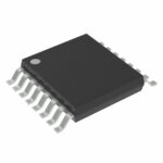 SN74HCS367PWR
SN74HCS367PWR is listed in the Buffers, Drivers, Receivers, Transceivers range at ChipApex. The manufacturer field lists Texas Instruments. Its product description is IC BUFFER…
Read More
SN74HCS367PWR is listed in the Buffers, Drivers, Receivers, Transceivers range at ChipApex. The manufacturer field lists Texas Instruments. Its product description is IC BUFFER…
Read More
Choose a DIP switch by contact type, coded positions, footprint and signal ratings. Check logic polarity, assembly conditions and PCB configuration behavior.
Read More
SN74HCS367PWR is listed in the Buffers, Drivers, Receivers, Transceivers range at ChipApex. The manufacturer field lists Texas Instruments. Its product description is IC BUFFER…
Read More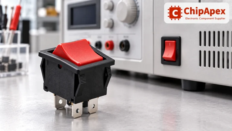
Choose a rocker switch by AC/DC ratings, contact arrangement, illumination, panel fit and sealing. Get practical checks for engineering and component sourcing.
Read More
See how a MEMS gyroscope measures angular rate, why its angle estimate drifts, and which range, noise, interface and temperature specs to compare.
Read More
SN74HCS367PWR is listed in the Buffers, Drivers, Receivers, Transceivers range at ChipApex. The manufacturer field lists Texas Instruments. Its product description is IC BUFFER…
Read More
SN74HCS367PWR is listed in the Buffers, Drivers, Receivers, Transceivers range at ChipApex. The manufacturer field lists Texas Instruments. Its product description is IC BUFFER…
Read More
SN74HCS367PWR is listed in the Buffers, Drivers, Receivers, Transceivers range at ChipApex. The manufacturer field lists Texas Instruments. Its product description is IC BUFFER…
Read More
SN74HCS367PWR is listed in the Buffers, Drivers, Receivers, Transceivers range at ChipApex. The manufacturer field lists Texas Instruments. Its product description is IC BUFFER…
Read More
SN74HCS367PWR is listed in the Buffers, Drivers, Receivers, Transceivers range at ChipApex. The manufacturer field lists Texas Instruments. Its product description is IC BUFFER…
Read More
SN74HCS367PWR is listed in the Buffers, Drivers, Receivers, Transceivers range at ChipApex. The manufacturer field lists Texas Instruments. Its product description is IC BUFFER…
Read More
The activity of extra discounts on wholesale prices is in full swing…
Please fill in your contact information and we will send you the latest wholesale price list.





