 ChipApex | Global Electronic Components Supplier

SEARCH
Search Product
Search Post
— IC芯片 | 连接器 | 传感器 | 被动器件 —
Search productSearch post
— IC芯片 | 连接器 | 传感器 | 被动器件 —
Consult the customer manager about the wholesale price.
consultation hotline:86-132-6715-2157
email:[email protected]
Contact the product manager for consultation. One-stop consultation is available.
Do you want a lower wholesale price? Please send us your inquiry and we will reply immediately.
SN74LS96D is listed in the Shift Registers range at ChipApex. The manufacturer field lists Texas Instruments. Its product description is PARALLEL IN PARALLEL OUT. Review the specifications below when checking this part for your BOM.
The SN74LS96D is a five-bit serial-in/serial-out shift register from the Texas Instruments SN74LS series. It features a dedicated clear input to reset all flip-flops and an output enable control for managing data flow. The device operates within a supply voltage range of 4.75 V to 5.25 V, with a typical propagation delay of 18 ns. It is housed in a 16-pin SOIC package and supports industrial temperature ranges.
Verify the specific suffix against the manufacturer's official documentation to confirm pinout compatibility and electrical characteristics. Ensure the component meets required environmental standards for the target application. Cross-reference the datasheet revision date to guarantee alignment with current design specifications.
Select this component when a simple five-bit shift register is required within standard TTL logic families. Consider the 18 ns propagation delay and 5 V operating voltage constraints. Evaluate package availability and thermal requirements for the intended PCB layout before finalizing the design.
This part belongs to the SN74LS family, known for low-power Schottky logic. It serves as a fundamental building block for sequential logic designs requiring temporary data storage or movement. The device complements other LS-series gates for complex digital system implementations.
Check for direct equivalents such as the SN74LS96N or SN74LS96J if package variations are acceptable. Verify functional compatibility with alternative manufacturers' parts before substitution.
The clear input asynchronously resets all five flip-flops to a low state, regardless of the clock or data inputs.
No, the SN74LS96D is a serial-in/serial-out shift register and does not feature parallel load capabilities.
Explore related parts through Logic, Integrated Circuits (ICs), all product categories, ChipApex homepage.
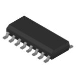 SN74LS96D
Choose LED drivers by current, string voltage, dimming and thermal limits. Understand constant-current operation and the checks needed for your load.
Read More
SN74LS96D is listed in the Shift Registers range at ChipApex. The manufacturer field lists Texas Instruments. Its product description is PARALLEL IN PARALLEL OUT.…
Read More
Compare variable capacitor types and varactor tuning. Understand capacitance-voltage curves, Q, bias and LC resonance before choosing a component.
Read More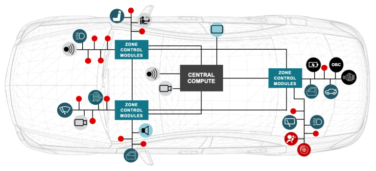
SN74LS96D is listed in the Shift Registers range at ChipApex. The manufacturer field lists Texas Instruments. Its product description is PARALLEL IN PARALLEL OUT.…
Read More
SN74LS96D is listed in the Shift Registers range at ChipApex. The manufacturer field lists Texas Instruments. Its product description is PARALLEL IN PARALLEL OUT.…
Read More
SN74LS96D is listed in the Shift Registers range at ChipApex. The manufacturer field lists Texas Instruments. Its product description is PARALLEL IN PARALLEL OUT.…
Read More
SN74LS96D is listed in the Shift Registers range at ChipApex. The manufacturer field lists Texas Instruments. Its product description is PARALLEL IN PARALLEL OUT.…
Read More
SN74LS96D is listed in the Shift Registers range at ChipApex. The manufacturer field lists Texas Instruments. Its product description is PARALLEL IN PARALLEL OUT.…
Read More
Understand voltage controlled oscillator tuning, phase noise and PLL operation. Check supply noise, output loading and requirements before selection.
Read More
Compare RC, crystal and MEMS oscillator circuits. Check ppm, jitter, load capacitance, startup margin and output compatibility before choosing a clock source.
Read More
SN74LS96D is listed in the Shift Registers range at ChipApex. The manufacturer field lists Texas Instruments. Its product description is PARALLEL IN PARALLEL OUT.…
Read More
Learn what a transistor does in a circuit. Compare switching and amplification, BJT and MOSFET drive, operating limits and practical component selection.
Read More
The activity of extra discounts on wholesale prices is in full swing…
Please fill in your contact information and we will send you the latest wholesale price list.





