 ChipApex | Global Electronic Components Supplier

SEARCH
Search Product
Search Post
— IC芯片 | 连接器 | 传感器 | 被动器件 —
Search productSearch post
— IC芯片 | 连接器 | 传感器 | 被动器件 —
Consult the customer manager about the wholesale price.
consultation hotline:86-132-6715-2157
email:[email protected]
Contact the product manager for consultation. One-stop consultation is available.
Do you want a lower wholesale price? Please send us your inquiry and we will reply immediately.
SN74LV125APWT is listed in the Buffers, Drivers, Receivers, Transceivers range at ChipApex. The manufacturer field lists Texas Instruments. Its product description is IC BUF NON-INVERT 5.5V 14TSSOP. Review the specifications below when checking this part for your BOM.
The SN74LV125APWT is a quadruple bus buffer gate manufactured by Texas Instruments, featuring non-inverting logic and three-state outputs. It operates within a supply voltage range of 2.0 V to 5.5 V and utilizes a TSSOP-14 surface-mount package. The device provides low output drive capability with maximum currents of ±16 mA for both high and low states. Propagation delay is specified at 16.5 ns under 2.5 V conditions with a 50 pF load. It supports an operating temperature range from -40°C to +85°C.
Verify the specific suffix 'W' corresponds to the TSSOP-14 package configuration required for your PCB layout. Confirm that the component meets RoHS compliance standards if mandated by your manufacturing regulations. Ensure the ordering quantity aligns with the available tape-and-reel packaging options provided by the manufacturer or authorized distributors.
Select this component when a quad buffer with three-state functionality is required for bidirectional bus architectures. The LV series offers lower power consumption compared to older LVC or HC families while maintaining similar speed characteristics. Consider the TSSOP-14 package dimensions during thermal analysis and board space allocation to ensure proper heat dissipation and mechanical fit.
This part belongs to the SN74LV family of low-voltage CMOS logic devices. It serves as a fundamental building block for digital systems requiring signal isolation or level shifting between different voltage domains. The quadruple configuration allows for efficient integration in complex circuit designs where multiple signal paths need simultaneous buffering and control.
The output enable pin controls the three-state condition of the buffers. When asserted, it places the outputs in a high-impedance state, effectively disconnecting them from the bus to prevent signal contention.
Yes, the SN74LV125APWT operates within a supply voltage range of 2.0 V to 5.5 V, making it fully compatible with 3.3 V logic systems.
Explore related parts through Logic, Integrated Circuits (ICs), all product categories, ChipApex homepage.
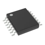 SN74LV125APWT

SN74LV125APWT is listed in the Buffers, Drivers, Receivers, Transceivers range at ChipApex. The manufacturer field lists Texas Instruments. Its product description is IC BUF…
Read More
Choose a rocker switch by AC/DC ratings, contact arrangement, illumination, panel fit and sealing. Get practical checks for engineering and component sourcing.
Read More
Choose a vibration sensor for machine monitoring. Compare sensing methods, bandwidth, noise and mounting, then define the signal-chain requirements.
Read More
SN74LV125APWT is listed in the Buffers, Drivers, Receivers, Transceivers range at ChipApex. The manufacturer field lists Texas Instruments. Its product description is IC BUF…
Read More
SN74LV125APWT is listed in the Buffers, Drivers, Receivers, Transceivers range at ChipApex. The manufacturer field lists Texas Instruments. Its product description is IC BUF…
Read More
SN74LV125APWT is listed in the Buffers, Drivers, Receivers, Transceivers range at ChipApex. The manufacturer field lists Texas Instruments. Its product description is IC BUF…
Read More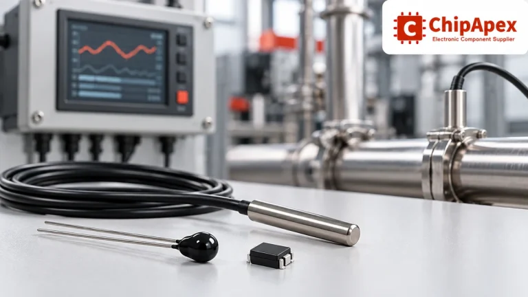
Compare thermistors, RTDs, thermocouples and temperature ICs. Learn how range, accuracy, response, interfaces and mounting affect component selection.
Read More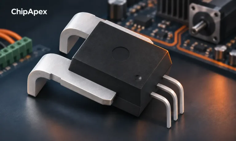
Compare Hall, shunt, current transformer and Rogowski sensing. Check AC/DC capability, accuracy, isolation, heat and response before selecting a sensor.
Read More
SN74LV125APWT is listed in the Buffers, Drivers, Receivers, Transceivers range at ChipApex. The manufacturer field lists Texas Instruments. Its product description is IC BUF…
Read More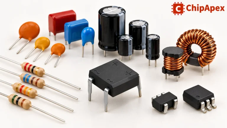
Explore electronic component types, functions, packages and datasheets. Learn selection, replacement and BOM checks before ordering parts for your PCB.
Read More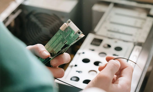
SN74LV125APWT is listed in the Buffers, Drivers, Receivers, Transceivers range at ChipApex. The manufacturer field lists Texas Instruments. Its product description is IC BUF…
Read More
Compare gas sensor technologies, cross-sensitivity and calibration needs. Define the gas, range and environment before choosing a sensing component.
Read More
The activity of extra discounts on wholesale prices is in full swing…
Please fill in your contact information and we will send you the latest wholesale price list.





