 ChipApex | Global Electronic Components Supplier

SEARCH
Search Product
Search Post
— IC芯片 | 连接器 | 传感器 | 被动器件 —
Search productSearch post
— IC芯片 | 连接器 | 传感器 | 被动器件 —
Consult the customer manager about the wholesale price.
consultation hotline:86-132-6715-2157
email:[email protected]
Contact the product manager for consultation. One-stop consultation is available.
Do you want a lower wholesale price? Please send us your inquiry and we will reply immediately.
SN74LVC125ADG4 is listed in the Buffers, Drivers, Receivers, Transceivers range at ChipApex. The manufacturer field lists Texas Instruments. Its product description is IC BUF NON-INVERT 3.6V 14SOIC. Review the specifications below when checking this part for your BOM.
The SN74LVC125ADG4 is a quadruple bus buffer gate with 3-state outputs manufactured by Texas Instruments. It operates from 1.65V to 3.6V and features independent output-enable inputs for each buffer. The device accepts input voltages up to 5.5V, enabling voltage translation in mixed 3.3V/5V systems. It is specified for operation from -40°C to 85°C and -40°C to 125°C. The maximum propagation delay is 4.8ns at 3.3V. Typical output ground bounce is 2V at VCC = 3.3V. Latch-up performance exceeds 250mA per JESD 17. It is housed in a 14-pin SOIC package.
Verify the specific ordering suffix 'DG4' corresponds to the RoHS-compliant lead finish (NIPDAU) and tube packaging configuration. Confirm the operating temperature range requirements match the datasheet specifications of -40°C to 85°C or -40°C to 125°C. Ensure the design accounts for the recommended bypass capacitor placement near the VCC pin to prevent power disturbances during operation.
Select this component when a quadruple non-inverting buffer with high-impedance states is required for 1.65V to 3.6V logic systems. It is suitable for applications needing voltage translation between 3.3V and 5V domains due to its 5.5V tolerant inputs. Consider the SOIC-14 package dimensions and thermal resistance values if board space or heat dissipation are critical constraints in the layout.
This part belongs to the SN74LVC125A family of quadruple bus buffer gates. The 'DG4' suffix indicates a specific manufacturing variant within the Texas Instruments portfolio, typically denoting RoHS compliance and a specific lead finish. It shares functional characteristics with other members of the LVC series but differs in physical packaging and environmental certifications.
SN74LVC125AD
To ensure the high-impedance state during power up or power down, the OE input should be tied to VCC through a pullup resistor.
Latch-up performance exceeds 250mA per JESD 17 standard.
Explore related parts through Logic, Integrated Circuits (ICs), all product categories, ChipApex homepage.
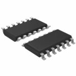 SN74LVC125ADG4
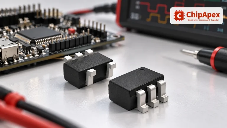
Choose logic inverter ICs by thresholds, supply, output drive and delay. Compare standard and Schmitt-trigger inputs, power sequencing and replacement checks.
Read More
SN74LVC125ADG4 is listed in the Buffers, Drivers, Receivers, Transceivers range at ChipApex. The manufacturer field lists Texas Instruments. Its product description is IC BUF…
Read More
SN74LVC125ADG4 is listed in the Buffers, Drivers, Receivers, Transceivers range at ChipApex. The manufacturer field lists Texas Instruments. Its product description is IC BUF…
Read More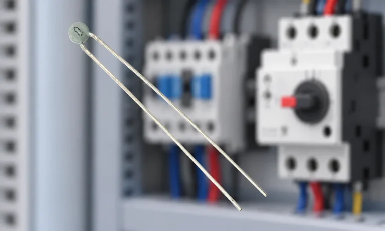
Learn why PTC resistance rises with temperature, how it differs from NTC, and which ratings matter for sensing and protection.
Read More
SN74LVC125ADG4 is listed in the Buffers, Drivers, Receivers, Transceivers range at ChipApex. The manufacturer field lists Texas Instruments. Its product description is IC BUF…
Read More
SN74LVC125ADG4 is listed in the Buffers, Drivers, Receivers, Transceivers range at ChipApex. The manufacturer field lists Texas Instruments. Its product description is IC BUF…
Read More
Choose an AC to DC converter by input range, output demand, isolation, efficiency and thermal derating. Compare architectures and check installation needs.
Read More
SN74LVC125ADG4 is listed in the Buffers, Drivers, Receivers, Transceivers range at ChipApex. The manufacturer field lists Texas Instruments. Its product description is IC BUF…
Read More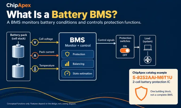
Learn what a battery BMS does, how protection differs from charging, and which pack specifications to check when sourcing BMS components through ChipApex.
Read More
SN74LVC125ADG4 is listed in the Buffers, Drivers, Receivers, Transceivers range at ChipApex. The manufacturer field lists Texas Instruments. Its product description is IC BUF…
Read More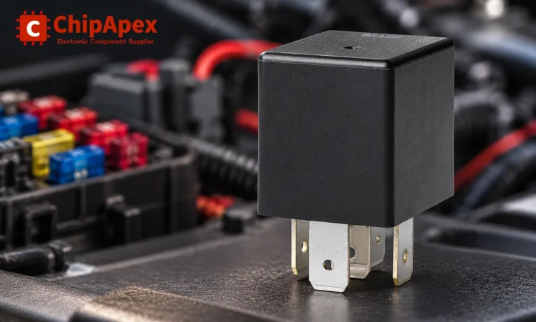
Learn the relay definition, coil and contact operation, NO and NC forms, load ratings and suppression choices. Compare mechanical, reed and solid-state types.
Read More
SN74LVC125ADG4 is listed in the Buffers, Drivers, Receivers, Transceivers range at ChipApex. The manufacturer field lists Texas Instruments. Its product description is IC BUF…
Read More
The activity of extra discounts on wholesale prices is in full swing…
Please fill in your contact information and we will send you the latest wholesale price list.





