 ChipApex | Global Electronic Components Supplier

SEARCH
Search Product
Search Post
— IC芯片 | 连接器 | 传感器 | 被动器件 —
Search productSearch post
— IC芯片 | 连接器 | 传感器 | 被动器件 —
Consult the customer manager about the wholesale price.
consultation hotline:86-132-6715-2157
email:[email protected]
Contact the product manager for consultation. One-stop consultation is available.
Do you want a lower wholesale price? Please send us your inquiry and we will reply immediately.
SN74LVC828APW is listed in the Buffers, Drivers, Receivers, Transceivers range at ChipApex. The manufacturer field lists Texas Instruments. Its product description is IC BUFFER INVERT 3.6V 24TSSOP. Review the specifications below when checking this part for your BOM.
The SN74LVC828APW is a 10-bit buffer and bus driver with 3-state outputs manufactured by Texas Instruments. It operates from a supply voltage range of 1.65 V to 3.6 V. The device provides inverting data at its outputs and features two active-low output-enable inputs (OE1, OE2) that function as a 2-input AND gate; if either input is high, all ten outputs enter a high-impedance state. It supports mixed-mode signal operation, allowing 5-V input/output voltage compatibility while powered by a 3.3-V VCC. The package is TSSOP-24.
Verify the specific ordering suffix 'PW' corresponds to the TSSOP package with a tube quantity of 60 units. Confirm the operating temperature range is -40°C to +85°C. Ensure the RoHS status and lead finish match project requirements. Check for any recent Product Change Notices affecting availability or specifications.
Select this component when a 10-bit inverting buffer with 3-state control is required for low-voltage logic applications. The LVC series ensures compatibility with standard CMOS logic levels. Verify that the maximum propagation delay meets the timing constraints of the target bus architecture. Consider the thermal impedance characteristics of the TSSOP package for the intended enclosure design.
This part belongs to the SN74LVC828A family of 10-bit buffers/drivers. It is designed for high-performance bus interface applications requiring wide data paths. The device is distinct from non-inverting buffers or single-ended drivers due to its specific 10-bit width and dual enable functionality.
SN74LVC828ADW (SOIC Package)
The SN74LVC828APW includes Ioff circuitry that automatically disables the outputs when the device is powered down, preventing damaging current backflow through the device.
The OE1 and OE2 inputs act as a 2-input AND gate with active-low polarity. If either OE1 or OE2 is high, all ten outputs are placed in the high-impedance state.
Explore related parts through Logic, Integrated Circuits (ICs), all product categories, ChipApex homepage.
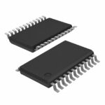 SN74LVC828APW
Select MOV varistors by continuous voltage, clamping behavior, surge waveform and repetition. Check thermal disconnection, fuse coordination and replacements.
Read More
SN74LVC828APW is listed in the Buffers, Drivers, Receivers, Transceivers range at ChipApex. The manufacturer field lists Texas Instruments. Its product description is IC BUFFER…
Read More
SN74LVC828APW is listed in the Buffers, Drivers, Receivers, Transceivers range at ChipApex. The manufacturer field lists Texas Instruments. Its product description is IC BUFFER…
Read More
SN74LVC828APW is listed in the Buffers, Drivers, Receivers, Transceivers range at ChipApex. The manufacturer field lists Texas Instruments. Its product description is IC BUFFER…
Read More
Select power transformers by input frequency, secondary VA, rectifier load, isolation, regulation and inrush. Build a clearer specification for your next RFQ.
Read More
SN74LVC828APW is listed in the Buffers, Drivers, Receivers, Transceivers range at ChipApex. The manufacturer field lists Texas Instruments. Its product description is IC BUFFER…
Read More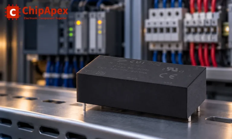
Choose an AC to DC converter by input range, output demand, isolation, efficiency and thermal derating. Compare architectures and check installation needs.
Read More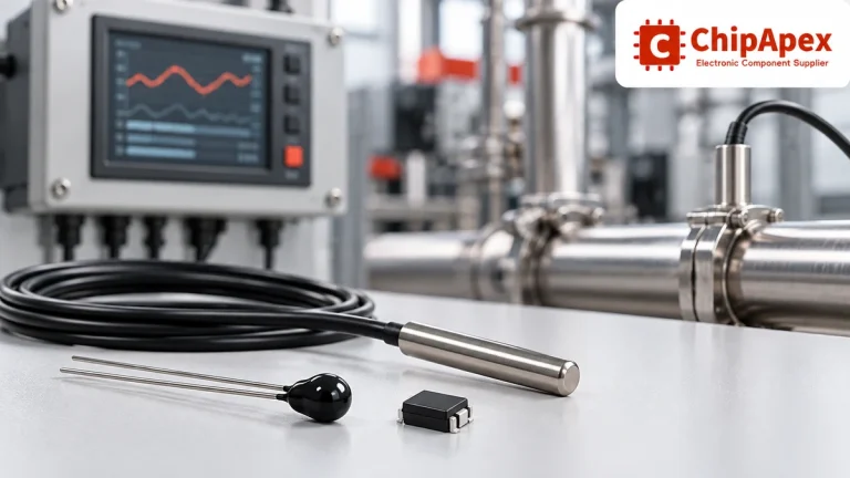
Compare thermistors, RTDs, thermocouples and temperature ICs. Learn how range, accuracy, response, interfaces and mounting affect component selection.
Read More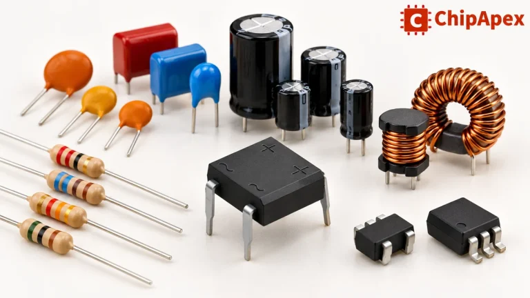
Explore electronic component types, functions, packages and datasheets. Learn selection, replacement and BOM checks before ordering parts for your PCB.
Read More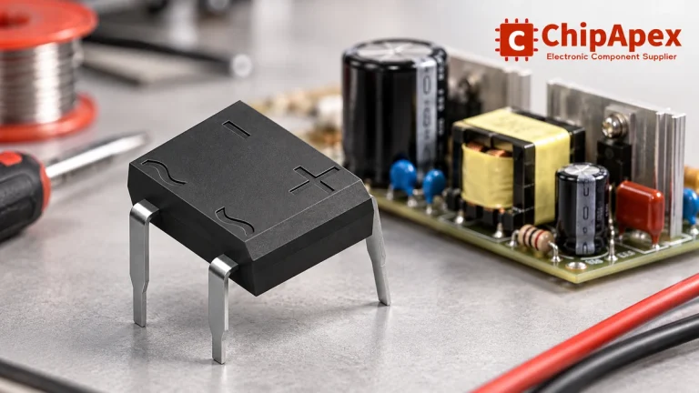
Select a bridge rectifier by reverse voltage, capacitor charging current, startup surge and cooling. Work through a stated DC voltage and ripple example.
Read More
SN74LVC828APW is listed in the Buffers, Drivers, Receivers, Transceivers range at ChipApex. The manufacturer field lists Texas Instruments. Its product description is IC BUFFER…
Read More
SN74LVC828APW is listed in the Buffers, Drivers, Receivers, Transceivers range at ChipApex. The manufacturer field lists Texas Instruments. Its product description is IC BUFFER…
Read More
The activity of extra discounts on wholesale prices is in full swing…
Please fill in your contact information and we will send you the latest wholesale price list.





