 ChipApex | Global Electronic Components Supplier

SEARCH
Search Product
Search Post
— IC芯片 | 连接器 | 传感器 | 被动器件 —
Search productSearch post
— IC芯片 | 连接器 | 传感器 | 被动器件 —
Consult the customer manager about the wholesale price.
consultation hotline:86-132-6715-2157
email:[email protected]
Contact the product manager for consultation. One-stop consultation is available.
Do you want a lower wholesale price? Please send us your inquiry and we will reply immediately.
SN74LVCH16244ADGG is listed in the Buffers, Drivers, Receivers, Transceivers range at ChipApex. The manufacturer field lists Texas Instruments. Its product description is IC BUFF NON-INVERT 3.6V 48TSSOP. Review the specifications below when checking this part for your BOM.
The SN74LVCH16244ADGG is a 16-bit buffer and line driver with 3-state outputs manufactured by Texas Instruments. It operates within a supply voltage range of 1.65 V to 3.6 V and features inputs tolerant up to 5.5 V, facilitating mixed-mode signal operation. The device provides a maximum propagation delay of 4.1 ns at 3.3 V and includes active bus-hold circuitry on data inputs. It supports partial-power-down modes via Ioff circuitry for back-drive protection and live insertion. The component is housed in a 48-pin TSSOP package.
Verify the specific ordering suffix against the manufacturer's current Package Option Addendum to confirm the exact physical package type and moisture sensitivity level. Ensure that the selected variant matches the required lead finish and reflow temperature profile for the intended assembly process. Cross-reference the part marking code to validate authenticity and traceability during the procurement phase.
Select this component when designing systems requiring 16-bit buffering with mixed-voltage compatibility between 3.3-V and 5-V logic domains. The device is suitable for applications needing high-density bus drivers with low power consumption. Consider the 4.1 ns propagation delay for timing-critical paths. Verify that the thermal resistance characteristics of the TSSOP package align with the system's heat dissipation requirements.
This device belongs to the Widebus family of logic components designed for high-performance digital applications. It serves as a non-inverting buffer/driver capable of driving memory address buses, clock signals, and bus-oriented receivers. The architecture allows configuration as four 4-bit buffers, two 8-bit buffers, or one single 16-bit buffer depending on the enable pin usage.
SN74LVCH16244ADL
The SN74LVCH16244A features active bus-hold circuitry that holds unused or undriven inputs at a valid logic state, eliminating the need for external pullup or pulldown resistors.
The Ioff circuitry disables the outputs when the device is powered down, preventing damaging current backflow through the device. This supports partial-power-down applications and live insertion.
Yes, the inputs accept voltages up to 5.5 V while the device operates from 1.65 V to 3.6 V, allowing it to be used as a translator in mixed 3.3-V/5-V system environments.
Explore related parts through Logic, Integrated Circuits (ICs), all product categories, ChipApex homepage.
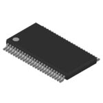 SN74LVCH16244ADGG
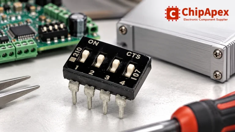
Choose a DIP switch by contact type, coded positions, footprint and signal ratings. Check logic polarity, assembly conditions and PCB configuration behavior.
Read More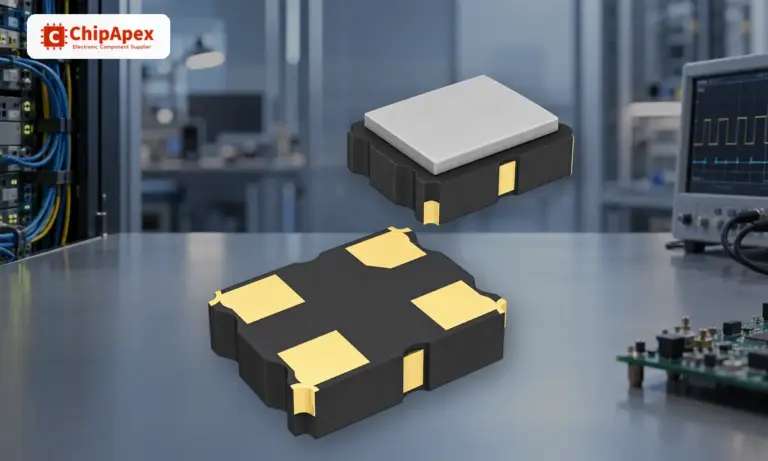
Understand how oscillators generate timing signals, how they differ from crystals, and which frequency, output and stability specs matter when choosing one.
Read More
SN74LVCH16244ADGG is listed in the Buffers, Drivers, Receivers, Transceivers range at ChipApex. The manufacturer field lists Texas Instruments. Its product description is IC BUFF…
Read More
SN74LVCH16244ADGG is listed in the Buffers, Drivers, Receivers, Transceivers range at ChipApex. The manufacturer field lists Texas Instruments. Its product description is IC BUFF…
Read More
Learn how a pressure transducer converts pressure into voltage, current, or digital output, and compare pressure references and key selection specs.
Read More
SN74LVCH16244ADGG is listed in the Buffers, Drivers, Receivers, Transceivers range at ChipApex. The manufacturer field lists Texas Instruments. Its product description is IC BUFF…
Read More
SN74LVCH16244ADGG is listed in the Buffers, Drivers, Receivers, Transceivers range at ChipApex. The manufacturer field lists Texas Instruments. Its product description is IC BUFF…
Read More
SN74LVCH16244ADGG is listed in the Buffers, Drivers, Receivers, Transceivers range at ChipApex. The manufacturer field lists Texas Instruments. Its product description is IC BUFF…
Read More
SN74LVCH16244ADGG is listed in the Buffers, Drivers, Receivers, Transceivers range at ChipApex. The manufacturer field lists Texas Instruments. Its product description is IC BUFF…
Read More
SN74LVCH16244ADGG is listed in the Buffers, Drivers, Receivers, Transceivers range at ChipApex. The manufacturer field lists Texas Instruments. Its product description is IC BUFF…
Read More
SN74LVCH16244ADGG is listed in the Buffers, Drivers, Receivers, Transceivers range at ChipApex. The manufacturer field lists Texas Instruments. Its product description is IC BUFF…
Read More
SN74LVCH16244ADGG is listed in the Buffers, Drivers, Receivers, Transceivers range at ChipApex. The manufacturer field lists Texas Instruments. Its product description is IC BUFF…
Read More
The activity of extra discounts on wholesale prices is in full swing…
Please fill in your contact information and we will send you the latest wholesale price list.





