 ChipApex | Global Electronic Components Supplier

SEARCH
Search Product
Search Post
— IC芯片 | 连接器 | 传感器 | 被动器件 —
Search productSearch post
— IC芯片 | 连接器 | 传感器 | 被动器件 —
Consult the customer manager about the wholesale price.
consultation hotline:86-132-6715-2157
email:[email protected]
Contact the product manager for consultation. One-stop consultation is available.
Do you want a lower wholesale price? Please send us your inquiry and we will reply immediately.
SY89828LHI is listed in the Clock Buffers, Drivers range at ChipApex. The manufacturer field lists Microchip Technology. Its product description is IC CLK BUFFER 2:10 1GHZ 64TQFP. Review the specifications below when checking this part for your BOM.
The SY89828LHI is a dual 1:10 LVDS fanout buffer and translator manufactured by Micrel, Inc. It operates on a single 3.3V supply and provides two banks of ten differential LVDS outputs. The device features a 2:1 input multiplexer for each bank, accepting either LVDS or LVPECL signals. Key electrical specifications include a maximum toggle frequency (fMAX) of 1.0 GHz, within-device skew under 50 ps, cycle-to-cycle jitter below 1 ps RMS, and total peak-to-peak jitter under 1 ps. Propagation delay ranges from 0.8 ns to 1.6 ns depending on the input type and amplitude.
Verify component authenticity through authorized channels as this part was originally produced by Micrel, Inc. before its acquisition by Microchip Technology. Confirm that the specific ordering suffix matches the required lead finish (Sn-Pb or Matte-Sn). Ensure PCB design accommodates the exposed pad thermal requirements for the H64-1 package.
Select the SY89828LHI when a high-density 20-output LVDS distribution solution is required with precise timing alignment. This model supports both LVDS and LVPECL inputs via internal multiplexing, eliminating the need for external level shifters. Verify that the application environment remains within the industrial temperature range (-40°C to +85°C) specified for this variant.
This component belongs to the Precision Edge series of high-performance clock buffers. Originally developed by Micrel, Inc., it serves as a specialized interface for translating and distributing low-voltage differential signals in high-speed digital systems requiring minimal phase noise and skew across multiple loads.
Publicly confirmed substitute part numbers are not available in the provided documentation. Designers should consult current Microchip Technology product portfolios for modern equivalents if new procurement is required.
The OE1 and OE2 inputs disable the outputs only when they are already in the LOW state. This synchronization prevents the generation of runt clock pulses that can occur with asynchronous control during enable/disable transitions.
LVDS inputs (LVDS_CLKA/B) have an internal 100Ω termination resistor. LVPECL inputs (LVPECL_CLKA/B) require external termination and utilize internal 75kΩ pull-down resistors when not selected.
Unused output pairs must be terminated with a 100Ω resistor to maintain low jitter and skew performance. When disabled, Q outputs remain static LOW and /Q outputs remain static HIGH.
Explore related parts through Clock/Timing, Integrated Circuits (ICs), all product categories, ChipApex homepage.
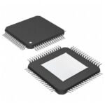 SY89828LHI

SY89828LHI is listed in the Clock Buffers, Drivers range at ChipApex. The manufacturer field lists Microchip Technology. Its product description is IC CLK BUFFER…
Read More
SY89828LHI is listed in the Clock Buffers, Drivers range at ChipApex. The manufacturer field lists Microchip Technology. Its product description is IC CLK BUFFER…
Read More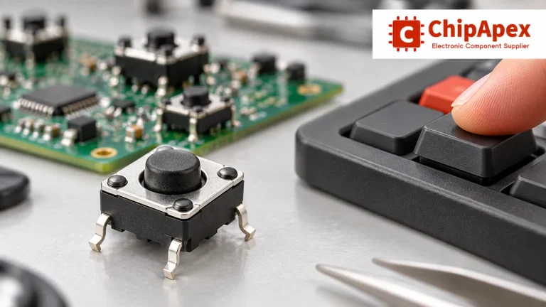
Understand tactile switches, PCB and keyboard differences, four-pin wiring, debounce, force, travel and replacement checks for reliable control inputs.
Read More
SY89828LHI is listed in the Clock Buffers, Drivers range at ChipApex. The manufacturer field lists Microchip Technology. Its product description is IC CLK BUFFER…
Read MoreSY89828LHI is listed in the Clock Buffers, Drivers range at ChipApex. The manufacturer field lists Microchip Technology. Its product description is IC CLK BUFFER…
Read More
SY89828LHI is listed in the Clock Buffers, Drivers range at ChipApex. The manufacturer field lists Microchip Technology. Its product description is IC CLK BUFFER…
Read More
SY89828LHI is listed in the Clock Buffers, Drivers range at ChipApex. The manufacturer field lists Microchip Technology. Its product description is IC CLK BUFFER…
Read More
SY89828LHI is listed in the Clock Buffers, Drivers range at ChipApex. The manufacturer field lists Microchip Technology. Its product description is IC CLK BUFFER…
Read More
SY89828LHI is listed in the Clock Buffers, Drivers range at ChipApex. The manufacturer field lists Microchip Technology. Its product description is IC CLK BUFFER…
Read More
SY89828LHI is listed in the Clock Buffers, Drivers range at ChipApex. The manufacturer field lists Microchip Technology. Its product description is IC CLK BUFFER…
Read More
Learn how rectifiers convert AC to DC, compare half-wave and bridge circuits, and select voltage, current, recovery and thermal ratings for your design.
Read More
SY89828LHI is listed in the Clock Buffers, Drivers range at ChipApex. The manufacturer field lists Microchip Technology. Its product description is IC CLK BUFFER…
Read More
The activity of extra discounts on wholesale prices is in full swing…
Please fill in your contact information and we will send you the latest wholesale price list.







