ChipApex | Global Electronic Components Supplier

SEARCH
Search Product
Search Post
— IC芯片 | 连接器 | 传感器 | 被动器件 —
Search productSearch post
— IC芯片 | 连接器 | 传感器 | 被动器件 —
Consult the customer manager about the wholesale price.
consultation hotline:86-132-6715-2157
email:[email protected]
Contact the product manager for consultation. One-stop consultation is available.
Do you want a lower wholesale price? Please send us your inquiry and we will reply immediately.
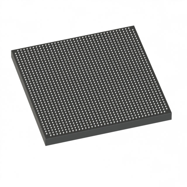
5SGSMD5K3F40C2 is listed in the Field Programmable Gate Array range at ChipApex. The manufacturer field lists Altera. Its product description is IC FPGA 696 I/O 1517FBGA. Review the specifications below when checking this part for your BOM.
The Altera 5SGSMD5K3F40C2LG is a Stratix V GS Field Programmable Gate Array featuring 457,000 logic elements and 172,600 Adaptive Logic Modules. It integrates 39 Mbit of embedded memory and supports up to 696 I/Os within a 1517-ball FCBGA package. The device operates with core voltages between 0.82V and 0.88V, supporting data rates up to 14.1 Gb/s via integrated transceivers. It functions within a junction temperature range of 0°C to 85°C.
Verify the complete part number, as suffixes such as LG or C2 indicate specific packaging, temperature, or speed grades. Confirm RoHS compliance status and moisture sensitivity level requirements for your assembly process. Check current availability as distribution channels may vary. Ensure compatibility with Quartus software versions supported by this device generation.
Select based on required logic density and I/O count relative to the 457,000 LE capacity. Evaluate power consumption profiles against available cooling solutions for the 1517-ball package. Consider thermal management needs given the 85°C maximum junction temperature limit. Verify that the selected speed grade meets timing constraints for target clock frequencies.
This component belongs to the Intel (formerly Altera) Stratix V family, representing a 28-nm technology node. It targets high-performance applications requiring substantial parallel processing capabilities. The GS variant typically offers cost-effective performance compared to higher-end GTX or GX series devices while maintaining robust connectivity features.
Direct replacements within the same package footprint are limited due to specific pinout configurations. Upgrading to newer Intel FPGA families requires schematic and layout redesign. Cross-reference with other Stratix V variants only if electrical parameters and pin compatibility are explicitly verified in official documentation.
Explore related parts through Embedded, Integrated Circuits (ICs), all product categories, ChipApex homepage.

 5SGSMD5K3F40C2

5SGSMD5K3F40C2 is listed in the Field Programmable Gate Array range at ChipApex. The manufacturer field lists Altera. Its product description is IC FPGA 696…
Read More
5SGSMD5K3F40C2 is listed in the Field Programmable Gate Array range at ChipApex. The manufacturer field lists Altera. Its product description is IC FPGA 696…
Read More
Select a bridge rectifier by reverse voltage, capacitor charging current, startup surge and cooling. Work through a stated DC voltage and ripple example.
Read More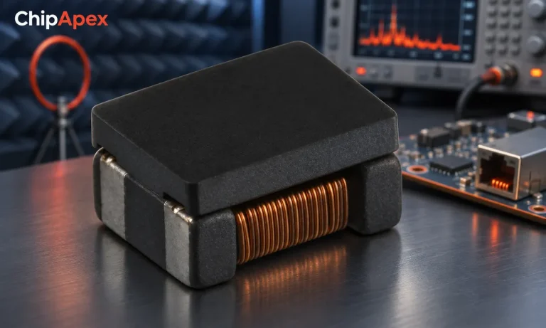
Select a common mode choke using noise frequency, current, insulation and signal integrity. Understand impedance curves, layout and filter limitations.
Read More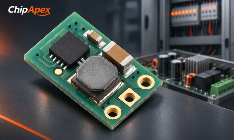
Select a DC-DC converter by input range, topology, isolation and temperature. Compare ripple, efficiency and load limits before choosing a component.
Read More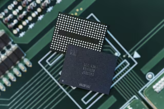
5SGSMD5K3F40C2 is listed in the Field Programmable Gate Array range at ChipApex. The manufacturer field lists Altera. Its product description is IC FPGA 696…
Read More
Learn what data acquisition means, from sensors and conditioning to sampling and storage. Review channel timing, wiring, calibration and data quality.
Read More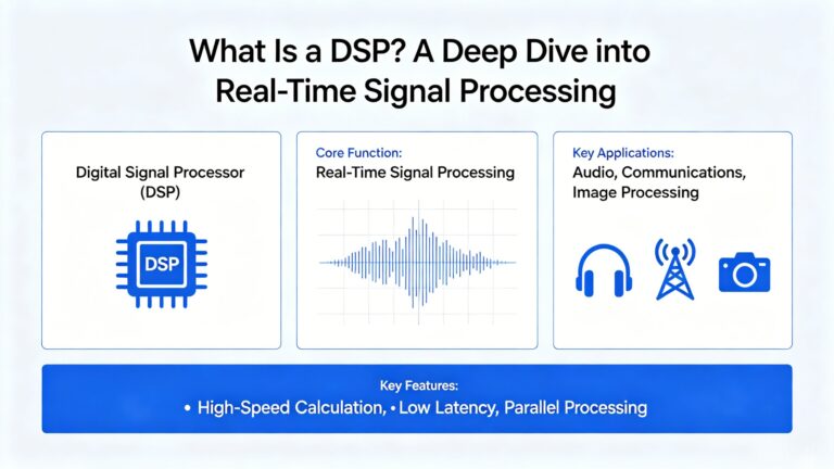
5SGSMD5K3F40C2 is listed in the Field Programmable Gate Array range at ChipApex. The manufacturer field lists Altera. Its product description is IC FPGA 696…
Read More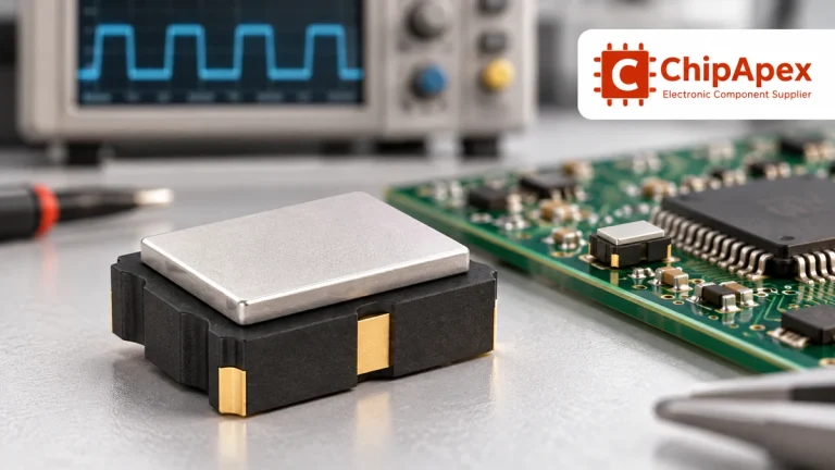
Compare RC, crystal and MEMS oscillator circuits. Check ppm, jitter, load capacitance, startup margin and output compatibility before choosing a clock source.
Read More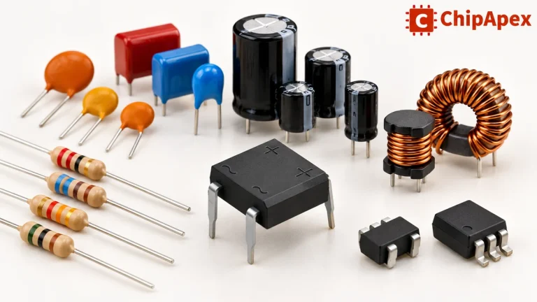
Explore electronic component types, functions, packages and datasheets. Learn selection, replacement and BOM checks before ordering parts for your PCB.
Read More
5SGSMD5K3F40C2 is listed in the Field Programmable Gate Array range at ChipApex. The manufacturer field lists Altera. Its product description is IC FPGA 696…
Read More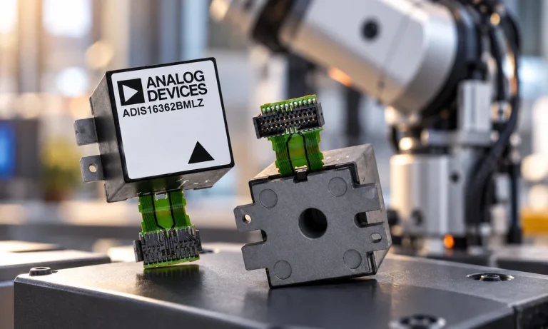
Learn what an IMU measures, how accelerometers and gyroscopes work together, why orientation estimates drift, and what to compare.
Read More
The activity of extra discounts on wholesale prices is in full swing…
Please fill in your contact information and we will send you the latest wholesale price list.