 ChipApex | Global Electronic Components Supplier
71V2556SA100BGGI
Search Product
Search Post
— IC芯片 | 连接器 | 传感器 | 被动器件 —
Search productSearch post
— IC芯片 | 连接器 | 传感器 | 被动器件 —
Consult the customer manager about the wholesale price.
consultation hotline:86-132-6715-2157
email:[email protected]
Contact the product manager for consultation. One-stop consultation is available.
Do you want a lower wholesale price? Please send us your inquiry and we will reply immediately.
The 71V2556SA100BGGI is a 4.5 Mbit synchronous static random-access memory (SRAM) organized as 128K x 36. It operates with a 3.3V core supply and supports 2.5V I/O levels, functioning within a voltage range of 3.135V to 3.465V. The device features a maximum clock frequency of 100 MHz and an access time of 5 ns. It utilizes a parallel interface and is housed in a 119-pin PBGA package measuring 14x22 mm. Designed for industrial applications, it functions reliably between -40°C and +85°C.
Verify component authenticity through authorized channels due to End-of-Life status. Confirm moisture sensitivity level handling requirements before assembly. Check for RoHS compliance variations across manufacturing dates. Validate package markings against official datasheet specifications to ensure correct revision identification.
Select this component for designs requiring 36-bit data width and synchronous pipelined performance. Ensure system power supplies accommodate the specified 3.3V core and 2.5V I/O requirements. Verify that the PCB layout supports the 119-pin PBGA footprint and thermal dissipation needs for industrial temperature operation.
This part belongs to the Renesas 71V2556 series of Zero Bus Turnaround synchronous SRAMs. It shares architectural similarities with other members like the 71V2556S150PFGI8 but differs in speed grade and package type. The series is characterized by its ability to eliminate bus turnaround latency, making it suitable for high-throughput memory interfaces.
Public confirmed substitute part numbers include IDT71V2556SA100BGI. Verify electrical compatibility and pinout alignment before substitution. Note that alternative packages such as TQFP variants exist within the same family but require different footprints.
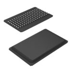 71V2556SA100BGGI
The activity of extra discounts on wholesale prices is in full swing…
Please fill in your contact information and we will send you the latest wholesale price list.





