 ChipApex | Global Electronic Components Supplier

SEARCH
Search Product
Search Post
— IC芯片 | 连接器 | 传感器 | 被动器件 —
Search productSearch post
— IC芯片 | 连接器 | 传感器 | 被动器件 —
Consult the customer manager about the wholesale price.
consultation hotline:86-132-6715-2157
email:[email protected]
Contact the product manager for consultation. One-stop consultation is available.
Do you want a lower wholesale price? Please send us your inquiry and we will reply immediately.
74AUP1T34GXXL is listed in the Buffers, Drivers, Receivers, Transceivers range at ChipApex. The manufacturer field lists Nexperia USA Inc.. Its product description is 74AUP1T34 - Low-power dual supp. Review the specifications below when checking this part for your BOM.
The Nexperia 74AUP1T34GXXL is a single dual-supply translating buffer from the 74AUP series. It features independent supply voltage ports, VCC(A) and VCC(Y), both operating within a range of 1.1 V to 3.6 V. The device provides Schmitt-trigger action for noise immunity and includes IOFF circuitry to prevent backflow current during partial power-down states. It supports an ambient temperature range of -40 °C to +125 °C and complies with JEDEC standards JESD8-7, JESD8-5, and JESD8-B.
Verify the specific package suffix corresponding to 'GXXL' against official Nexperia documentation, as standard listings typically use suffixes like GW or GX. Confirm that the requested variant matches the exact pinout and thermal characteristics defined in the product data sheet before finalizing procurement specifications.
Select this component when interfacing circuits with distinct supply voltages within the 1.1 V to 3.6 V range. Ensure the design accounts for the required propagation delay variations across different load capacitances and temperature conditions specified in the dynamic characteristics tables.
This device belongs to the 74AUP family of low-power CMOS logic devices. It serves as a specialized translator buffer, differing from standard buffers by its ability to operate with two separate supply rails. This makes it suitable for bridging gaps between subsystems powered by different voltage levels without external components.
The IOFF circuitry disables the output when the device is powered down, preventing potentially damaging backflow current through the device.
The input voltage can withstand up to 4.6 V, providing overvoltage tolerance even when the device is powered down.
Explore related parts through Logic, Integrated Circuits (ICs), all product categories, ChipApex homepage.
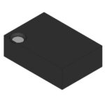 74AUP1T34GXXL
74AUP1T34GXXL is listed in the Buffers, Drivers, Receivers, Transceivers range at ChipApex. The manufacturer field lists Nexperia USA Inc.. Its product description is 74AUP1T34…
Read More
74AUP1T34GXXL is listed in the Buffers, Drivers, Receivers, Transceivers range at ChipApex. The manufacturer field lists Nexperia USA Inc.. Its product description is 74AUP1T34…
Read More
74AUP1T34GXXL is listed in the Buffers, Drivers, Receivers, Transceivers range at ChipApex. The manufacturer field lists Nexperia USA Inc.. Its product description is 74AUP1T34…
Read More
Choose a DIP switch by contact type, coded positions, footprint and signal ratings. Check logic polarity, assembly conditions and PCB configuration behavior.
Read More
74AUP1T34GXXL is listed in the Buffers, Drivers, Receivers, Transceivers range at ChipApex. The manufacturer field lists Nexperia USA Inc.. Its product description is 74AUP1T34…
Read More
74AUP1T34GXXL is listed in the Buffers, Drivers, Receivers, Transceivers range at ChipApex. The manufacturer field lists Nexperia USA Inc.. Its product description is 74AUP1T34…
Read More
74AUP1T34GXXL is listed in the Buffers, Drivers, Receivers, Transceivers range at ChipApex. The manufacturer field lists Nexperia USA Inc.. Its product description is 74AUP1T34…
Read More
74AUP1T34GXXL is listed in the Buffers, Drivers, Receivers, Transceivers range at ChipApex. The manufacturer field lists Nexperia USA Inc.. Its product description is 74AUP1T34…
Read More
74AUP1T34GXXL is listed in the Buffers, Drivers, Receivers, Transceivers range at ChipApex. The manufacturer field lists Nexperia USA Inc.. Its product description is 74AUP1T34…
Read More
74AUP1T34GXXL is listed in the Buffers, Drivers, Receivers, Transceivers range at ChipApex. The manufacturer field lists Nexperia USA Inc.. Its product description is 74AUP1T34…
Read More
Choose an AC to DC converter by input range, output demand, isolation, efficiency and thermal derating. Compare architectures and check installation needs.
Read More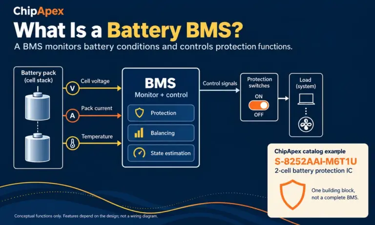
Learn what a battery BMS does, how protection differs from charging, and which pack specifications to check when sourcing BMS components through ChipApex.
Read More
The activity of extra discounts on wholesale prices is in full swing…
Please fill in your contact information and we will send you the latest wholesale price list.





