ChipApex | Global Electronic Components Supplier
9DBV0731AKLFT
Search Product
Search Post
— IC芯片 | 连接器 | 传感器 | 被动器件 —
Search productSearch post
— IC芯片 | 连接器 | 传感器 | 被动器件 —
Consult the customer manager about the wholesale price.
consultation hotline:86-132-6715-2157
email:[email protected]
Contact the product manager for consultation. One-stop consultation is available.
Do you want a lower wholesale price? Please send us your inquiry and we will reply immediately.
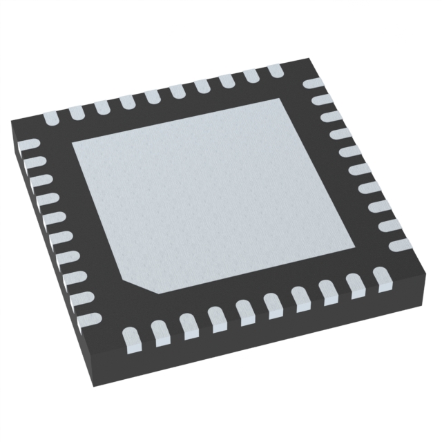
The 9DBV0731AKLFT is a seven-output, 1.8V PCIe fanout clock buffer manufactured by Renesas Electronics. Designed for PCI Express Gen 1 through 5 compliance, it features HCSL-compatible differential inputs and LP-HCSL differential outputs. The device supports frequencies from 1MHz to 200MHz and includes integrated 100Ω terminations for direct connection to transmission lines. It offers seven output enable pins for power management and three selectable SMBus addresses for configuration optimization.
Verify the suffix 'AKLFT' corresponds to the specific tape-and-reel packaging and lead-free composition required for the design. Confirm that the 1.8V supply voltage aligns with the target system's power rails. Ensure the 32-pin VFQFPN package dimensions fit the PCB footprint constraints. Check for RoHS compliance documentation if environmental regulations apply to the final assembly.
Select this component when a single HCSL source must drive up to seven PCIe loads with minimal board space. The integrated 100Ω terminations eliminate external resistors, saving approximately 46mm² compared to standard solutions. Choose this part over multiplexers if glitch-free switching between multiple sources is not required. Verify that the 250fs typical additive phase jitter meets the system's timing budget.
This device belongs to the 9DBV05x1-07x1-09x1 family of 1.8V PCIe fanout buffers. It shares architectural similarities with the 9DBV0541 (5-output) and 9DBV0941 (9-output) variants, differing primarily in output count and pin configuration. All members support SMBus control and spread spectrum input tolerance.
The 9DBV0541 serves as a lower-output alternative if fewer than seven drives are needed. The 9DBV0941 provides additional outputs for larger systems. For 3.3V applications, the 9DML04 series may be considered, though it functions as a multiplexer rather than a pure fanout buffer.
 9DBV0731AKLFT
The activity of extra discounts on wholesale prices is in full swing…
Please fill in your contact information and we will send you the latest wholesale price list.