 ChipApex | Global Electronic Components Supplier
9DML2855NDGI8
Search Product
Search Post
— IC芯片 | 连接器 | 传感器 | 被动器件 —
Search productSearch post
— IC芯片 | 连接器 | 传感器 | 被动器件 —
Consult the customer manager about the wholesale price.
consultation hotline:86-132-6715-2157
email:[email protected]
Contact the product manager for consultation. One-stop consultation is available.
Do you want a lower wholesale price? Please send us your inquiry and we will reply immediately.
The 9DML2855NDGI8 is a 2-input, 8-output clock multiplexer from Renesas Electronics, designed for PCIe Gen1–5 and legacy DB2000Q applications. It operates with an input frequency range of 1 MHz to 400 MHz and delivers LP-HCSL differential outputs. The device features low additive phase jitter (typical RMS 100 fs) and supports spread-spectrum inputs. Key functional attributes include Flexible Power Sequencing (FPS), Power Down Tolerant (PDT) ESD protection on inputs, and individual Output Enable (OE#) pins supporting PCIe CLKREQ#. It utilizes a 6mm × 6mm 48-VFQFPN package and functions within a -40 °C to +85 °C temperature range.
Verify the specific suffix 'NDGI8' against official Renesas documentation to confirm tape-and-reel packaging and industrial temperature grade (-40°C to +85°C). Ensure the ordering part number matches the exact pinout and electrical specifications required for the target design, as suffixes may indicate variations in shipping quantity or material compliance.
Select this component when designing for PCIe Gen1–5 standards requiring low additive jitter (<100 fs typical) and flexible power sequencing. It is suitable for complex clock topologies like SRIS and SRNS. Consider the 48-VFQFPN package size for board space constraints. Verify that the 3.3V supply voltage and HCSL input/LP-HCSL output signaling levels align with the system's logic families.
The 9DML2855 belongs to Renesas' family of clock multiplexers tailored for PCI Express applications. It addresses the need for low-jitter clock distribution in multi-lane interfaces. The NDGI8 variant specifically denotes the industrial temperature range and reel packaging configuration within the broader 9DML2855 product line.
Publicly confirmed substitute part numbers are not available in the provided reference data. Evaluate other Renesas PCIe clock muxes such as the 9DML04 for lower output count requirements or the 9ZML1255 for higher output counts, ensuring compatibility with PCIe generation and package constraints.
The provided documentation confirms Flexible Power Sequencing (FPS) and Power Down Tolerant (PDT) features but does not explicitly state glitch-free switching capability for the 9DML2855, unlike the 9DML04 which specifies selectable asynchronous or glitch-free modes.
The device accepts input frequencies ranging from 1 MHz to 400 MHz.
The 9DML2855 provides 8 differential outputs.
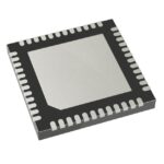 9DML2855NDGI8
The activity of extra discounts on wholesale prices is in full swing…
Please fill in your contact information and we will send you the latest wholesale price list.






