 ChipApex | Global Electronic Components Supplier
AD9523-1BCPZ-REEL7
Search Product
Search Post
— IC芯片 | 连接器 | 传感器 | 被动器件 —
Search productSearch post
— IC芯片 | 连接器 | 传感器 | 被动器件 —
Consult the customer manager about the wholesale price.
consultation hotline:86-132-6715-2157
email:[email protected]
Contact the product manager for consultation. One-stop consultation is available.
Do you want a lower wholesale price? Please send us your inquiry and we will reply immediately.
The AD9523-1BCPZ-REEL7 is a low jitter clock generator with 14 configurable outputs (LVPECL, LVDS, HSTL, LVCMOS) in a 72-LFCSP-VQ package. It features a dual PLL architecture with an integrated VCO tuning from 2.94 GHz to 3.1 GHz. The device supports input frequencies up to 400 MHz and output frequencies up to 1 GHz. Supply voltages range from 1.768 V to 3.465 V for logic/dividers and 3.135 V to 3.465 V for PLLs/drivers. Operating temperature spans -40°C to +85°C.
Verify the REEL7 suffix indicates tape-and-reel packaging. Confirm the B-grade designation matches required performance specifications. Ensure the 72-LFCSP-VQ footprint aligns with PCB layout guidelines. Check for moisture sensitivity level (MSL) requirements during storage and handling.
Select this component when low phase noise is critical for data converter SNR. Use the external VCXO connection via PLL1 for stringent jitter requirements. Verify that the 14-output count and configurable driver types (LVPECL/LVDS/HSTL/CMOS) meet system interface needs. Consider thermal dissipation if operating near maximum frequency and temperature limits.
This part belongs to the AD9523 series, designed for multi-output clock distribution with on-chip PLL and VCO capabilities. It serves as a key component in wireless infrastructure and high-performance instrumentation where precise timing alignment and low jitter are essential.
Public confirmed substitute part numbers are not available in the provided documentation. Evaluate pin-compatible alternatives within the Analog Devices portfolio only after verifying electrical parameter compatibility and software register mapping differences.
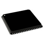 AD9523-1BCPZ-REEL7
The activity of extra discounts on wholesale prices is in full swing…
Please fill in your contact information and we will send you the latest wholesale price list.





