ChipApex | Global Electronic Components Supplier

SEARCH
Search Product
Search Post
— IC芯片 | 连接器 | 传感器 | 被动器件 —
Search productSearch post
— IC芯片 | 连接器 | 传感器 | 被动器件 —
Consult the customer manager about the wholesale price.
consultation hotline:86-132-6715-2157
email:[email protected]
Contact the product manager for consultation. One-stop consultation is available.
Do you want a lower wholesale price? Please send us your inquiry and we will reply immediately.
AD9642BCPZRL7-250 is listed in the Analog To Digital Converters (ADC) range at ChipApex. The manufacturer field lists Analog Devices Inc.. Its product description is IC ADC 14BIT PIPELINED 32LFCSP. Review the specifications below when checking this part for your BOM.
The AD9642BCPZRL7-250 is a 14-bit, high-speed analog-to-digital converter (ADC) from Analog Devices Inc., operating at a maximum sampling rate of 250 MSPS. It features a multistage differential pipelined architecture with integrated output error correction logic and an internal voltage reference. The device supports flexible analog input ranges from 1.4 V p-p to 2.0 V p-p and includes an ADC clock duty cycle stabilizer. It operates on single 1.8 V analog and digital supplies, consuming 390 mW at full speed. Data outputs are provided via DDR LVDS compliant with ANSI-644 levels. The component is housed in a 32-lead LFCSP package and is specified over the industrial temperature range of −40°C to +85°C.
Verify the specific ordering suffix RL7 against the manufacturer's current documentation to confirm reel packaging and tape-and-reel specifications. Ensure the selected speed grade matches the required sampling rate for the target application. Cross-reference the part number with official distributor catalogs to confirm availability and compliance with regional regulatory standards such as RoHS.
Select this component when a 14-bit resolution and 250 MSPS sampling rate are required for wideband signal acquisition. Consider the internal reference and duty cycle stabilizer if minimizing external components is a priority. Evaluate the LVDS output interface compatibility with downstream FPGA or DSP devices. Verify that the 32-lead LFCSP package dimensions fit within the available PCB real estate constraints.
The AD9642 belongs to a family of high-speed ADCs designed for communications infrastructure. It shares pin compatibility with the AD9634 and AD6672, facilitating migration between different resolution and speed grades. The device addresses the need for small size and low cost in multi-standard cellular base stations and portable instrumentation.
The AD9642BCPZRL7-210 offers identical functionality but operates at a maximum sampling rate of 210 MSPS. The AD9642BCPZRL7-170 provides a 170 MSPS option. These variants maintain pin compatibility and architectural similarities, allowing for potential substitution if lower bandwidth requirements exist.
The DCO (Data Clock Output) pins provide an LVDS clock signal derived from the input clock, synchronized with the data output for use by downstream receivers.
An integrated ADC clock duty cycle stabilizer (DCS) compensates for variations in the input clock duty cycle, ensuring consistent performance across different clock sources.
The device has a fixed pipeline delay (latency) of 10 cycles from the input clock edge to the corresponding data output.
Explore related parts through Data Acquisition, Integrated Circuits (ICs), all product categories, ChipApex homepage.
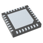 AD9642BCPZRL7-250

Choose a DIP switch by contact type, coded positions, footprint and signal ratings. Check logic polarity, assembly conditions and PCB configuration behavior.
Read More
AD9642BCPZRL7-250 is listed in the Analog To Digital Converters (ADC) range at ChipApex. The manufacturer field lists Analog Devices Inc.. Its product description is…
Read More
AD9642BCPZRL7-250 is listed in the Analog To Digital Converters (ADC) range at ChipApex. The manufacturer field lists Analog Devices Inc.. Its product description is…
Read More
AD9642BCPZRL7-250 is listed in the Analog To Digital Converters (ADC) range at ChipApex. The manufacturer field lists Analog Devices Inc.. Its product description is…
Read More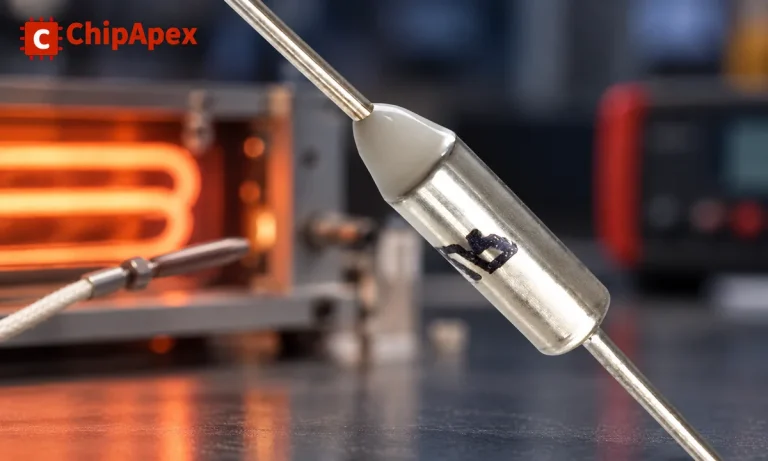
Understand thermal fuse operation, Tf, Th and Tm, electrical ratings and mounting. Check temperature limits and replacement requirements for your design.
Read More
AD9642BCPZRL7-250 is listed in the Analog To Digital Converters (ADC) range at ChipApex. The manufacturer field lists Analog Devices Inc.. Its product description is…
Read More
AD9642BCPZRL7-250 is listed in the Analog To Digital Converters (ADC) range at ChipApex. The manufacturer field lists Analog Devices Inc.. Its product description is…
Read More
AD9642BCPZRL7-250 is listed in the Analog To Digital Converters (ADC) range at ChipApex. The manufacturer field lists Analog Devices Inc.. Its product description is…
Read More
AD9642BCPZRL7-250 is listed in the Analog To Digital Converters (ADC) range at ChipApex. The manufacturer field lists Analog Devices Inc.. Its product description is…
Read More
AD9642BCPZRL7-250 is listed in the Analog To Digital Converters (ADC) range at ChipApex. The manufacturer field lists Analog Devices Inc.. Its product description is…
Read More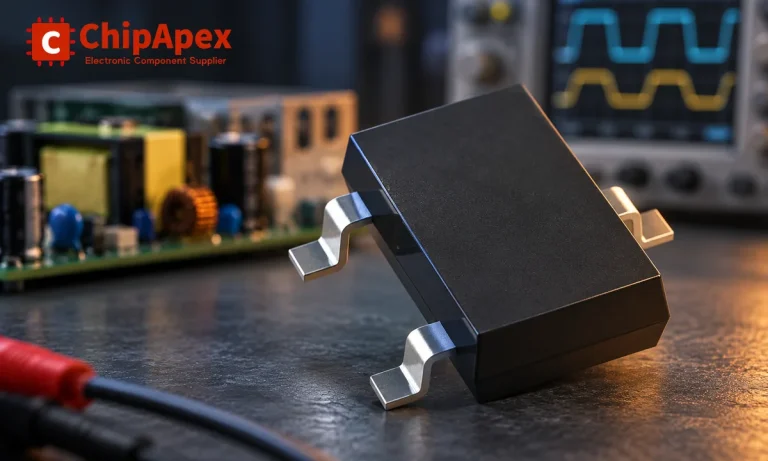
Learn how rectifiers convert AC to DC, compare half-wave and bridge circuits, and select voltage, current, recovery and thermal ratings for your design.
Read More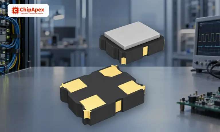
Understand how oscillators generate timing signals, how they differ from crystals, and which frequency, output and stability specs matter when choosing one.
Read More
The activity of extra discounts on wholesale prices is in full swing…
Please fill in your contact information and we will send you the latest wholesale price list.