 ChipApex | Global Electronic Components Supplier

SEARCH
Search Product
Search Post
— IC芯片 | 连接器 | 传感器 | 被动器件 —
Search productSearch post
— IC芯片 | 连接器 | 传感器 | 被动器件 —
Consult the customer manager about the wholesale price.
consultation hotline:86-132-6715-2157
email:[email protected]
Contact the product manager for consultation. One-stop consultation is available.
Do you want a lower wholesale price? Please send us your inquiry and we will reply immediately.
ADC10080CIMTX is listed in the Analog To Digital Converters (ADC) range at ChipApex. The manufacturer field lists Texas Instruments. Its product description is IC ADC 10BIT PIPELINED 28TSSOP. Review the specifications below when checking this part for your BOM.
The ADC10080CIMTX is a monolithic CMOS analog-to-digital converter featuring a pipeline architecture with digital error correction. It provides 10-bit resolution at an 80 MSPS conversion rate, consuming 78.6 mW at full speed and 15 mW in standby mode. The device operates on a single +3.0V supply and includes an on-chip sample-and-hold circuit and reference amplifier. It accepts differential or single-ended analog inputs with selectable full-scale swings of 2.0 VP-P, 1.5 VP-P, or 1.0 VP-P via the IRS pin. Output data formats are configurable as offset binary or two’s complement.
Verify the ordering suffix 'CIMTX' against the manufacturer's official documentation to confirm specific packaging details such as reel size or tape width. Confirm current production status and availability through authorized distributors, as older component families may have limited stock or end-of-life implications.
Ensure the analog supply voltage (VDDA) is maintained between +2.7V and +3.6V, while the digital supply (VDDIO) remains between +2.5V and VDDA. Maintain |VDDA–VDDIO| ≤ 100 mV for accuracy. Use separate bypass capacitors (0.1 µF and 4.7 µF) for each power supply pin. Verify that the clock frequency stays within the 20 MHz to 80 MHz range with a duty cycle between 30% and 70%.
The ADC10080CIMTX belongs to the ADC10080 family from Texas Instruments. It is housed in a 28-lead TSSOP package (Package Number PW). The device is designed for industrial temperature ranges (-40°C to +85°C) and utilizes a differential pipeline architecture to minimize power consumption while maintaining high dynamic performance.
Publicly confirmed substitute part numbers are not available in the provided source material. Consult the manufacturer's product selection guide for compatible alternatives with similar specifications.
The full-scale input swing is determined by the state of the IRS pin (Pin 5). Connecting IRS to VDDA selects 2.0 VP-P, connecting it to VSSA selects 1.5 VP-P, and leaving it floating selects 1.0 VP-P.
The ADC10080 has a conversion latency of 6 clock cycles due to its pipeline architecture. Data for any given sample is available at the output pins after the pipeline delay plus the output delay following the rising clock edge.
Yes. For single-ended operation, the VIN- pin (Pin 12) should be tied to the VCOM pin (Pin 4), and the input signal applied to VIN+ (Pin 13).
Explore related parts through Data Acquisition, Integrated Circuits (ICs), all product categories, ChipApex homepage.
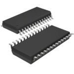 ADC10080CIMTX
 is listed in the Analog To Digital Converters (ADC) range at ChipApex. The manufacturer field lists Texas Instruments. Its product description is IC…
Read More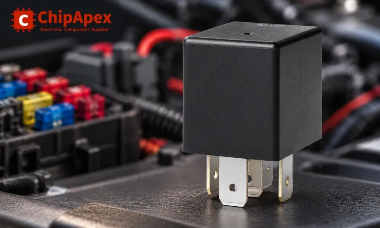
Learn the relay definition, coil and contact operation, NO and NC forms, load ratings and suppression choices. Compare mechanical, reed and solid-state types.
Read More
ADC10080CIMTX is listed in the Analog To Digital Converters (ADC) range at ChipApex. The manufacturer field lists Texas Instruments. Its product description is IC…
Read More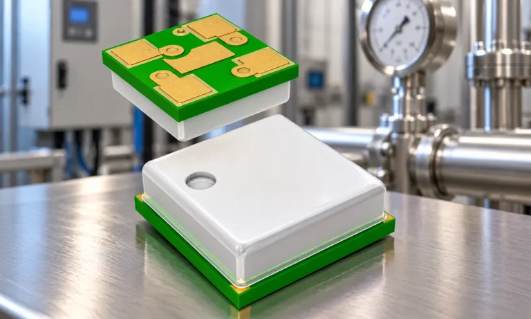
Learn how a pressure transducer converts pressure into voltage, current, or digital output, and compare pressure references and key selection specs.
Read More
ADC10080CIMTX is listed in the Analog To Digital Converters (ADC) range at ChipApex. The manufacturer field lists Texas Instruments. Its product description is IC…
Read More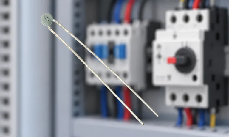
Learn why PTC resistance rises with temperature, how it differs from NTC, and which ratings matter for sensing and protection.
Read More
ADC10080CIMTX is listed in the Analog To Digital Converters (ADC) range at ChipApex. The manufacturer field lists Texas Instruments. Its product description is IC…
Read More
ADC10080CIMTX is listed in the Analog To Digital Converters (ADC) range at ChipApex. The manufacturer field lists Texas Instruments. Its product description is IC…
Read More
Select a bridge rectifier by reverse voltage, capacitor charging current, startup surge and cooling. Work through a stated DC voltage and ripple example.
Read More
ADC10080CIMTX is listed in the Analog To Digital Converters (ADC) range at ChipApex. The manufacturer field lists Texas Instruments. Its product description is IC…
Read More
ADC10080CIMTX is listed in the Analog To Digital Converters (ADC) range at ChipApex. The manufacturer field lists Texas Instruments. Its product description is IC…
Read More
Learn how a diode conducts, how to identify anode and cathode, and when to choose rectifier, TVS, Zener or photodiode types for a circuit.
Read More
The activity of extra discounts on wholesale prices is in full swing…
Please fill in your contact information and we will send you the latest wholesale price list.





