 ChipApex | Global Electronic Components Supplier

SEARCH
Search Product
Search Post
— IC芯片 | 连接器 | 传感器 | 被动器件 —
Search productSearch post
— IC芯片 | 连接器 | 传感器 | 被动器件 —
Consult the customer manager about the wholesale price.
consultation hotline:86-132-6715-2157
email:[email protected]
Contact the product manager for consultation. One-stop consultation is available.
Do you want a lower wholesale price? Please send us your inquiry and we will reply immediately.
ADG5423BCPZ-RL7 is listed in the Analog Switches, Multiplexers, Demultiplexers range at ChipApex. The manufacturer field lists Analog Devices Inc.. Its product description is IC SW SPST-NOX2 14OHM 10LFCSP. Review the specifications below when checking this part for your BOM.
The ADG5423BCPZ-RL7 is a dual single-pole/single-throw (SPST) analog switch from Analog Devices Inc., housed in a 10-lead Lead Frame Chip Scale Package (LFCSP). It operates with dual supplies of ±9 V to ±22 V or a single supply of 9 V to 40 V. Key electrical parameters include an on-resistance (RON) of 13.5 Ω typical at ±15 V, off-isolation of -55 dB, and a -3 dB bandwidth of 250 MHz. The device features latch-up immunity via trench isolation, an 8 kV HBM ESD rating, and break-before-make switching action.
Verify the component authenticity by checking the marking code BM on the package against the ordering guide. Confirm the suffix RL7 indicates tape and reel packaging. Ensure the temperature range matches the specified -40°C to +125°C for industrial applications. Cross-reference the datasheet revision A specifications with your design requirements.
Select the ADG5423 variant specifically when break-before-make switching is required for multiplexer applications to avoid transient shorts. Choose this part over the ADG5421 if asymmetric switch states are needed for Logic 1 inputs. Verify that the 13.5 Ω on-resistance meets the signal integrity requirements for the target voltage range.
This component belongs to the ADG54xx family of high-voltage, latch-up proof analog switches. It shares the same core architecture and pinout as the ADG5421 but differs in internal logic configuration. The family utilizes complementary metal oxide semiconductor (CMOS) technology designed for robust performance in harsh industrial environments.
The ADG5421BCPZ-RL7 is a logical substitute if break-before-make timing is not required, as it turns both switches on for a Logic 1 input. Other family members like the ADG5436 offer different switch configurations (SPDT) and should be evaluated for functional compatibility.
For a Logic 1 input, the ADG5421 turns both switches on, whereas the ADG5423 turns one switch on and the other off, providing break-before-make action.
It uses trench isolation, where a dielectric oxide layer separates the P-channel and N-channel transistors, eliminating the parasitic silicon-controlled rectifier circuit found in junction-isolated devices.
The absolute maximum rating for VDD to VSS is 48 V. Single-supply operation is supported up to 40 V, and dual-supply operation up to ±22 V.
Explore related parts through Interface, Integrated Circuits (ICs), all product categories, ChipApex homepage.
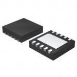 ADG5423BCPZ-RL7
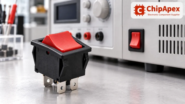
Choose a rocker switch by AC/DC ratings, contact arrangement, illumination, panel fit and sealing. Get practical checks for engineering and component sourcing.
Read More
ADG5423BCPZ-RL7 is listed in the Analog Switches, Multiplexers, Demultiplexers range at ChipApex. The manufacturer field lists Analog Devices Inc.. Its product description is IC…
Read More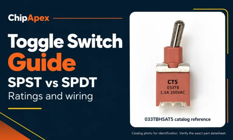
Compare SPST and SPDT toggle switches, understand AC/DC ratings, and follow wiring examples. Check contact action, mounting and parts in the ChipApex catalog.
Read More
ADG5423BCPZ-RL7 is listed in the Analog Switches, Multiplexers, Demultiplexers range at ChipApex. The manufacturer field lists Analog Devices Inc.. Its product description is IC…
Read More
ADG5423BCPZ-RL7 is listed in the Analog Switches, Multiplexers, Demultiplexers range at ChipApex. The manufacturer field lists Analog Devices Inc.. Its product description is IC…
Read More
ADG5423BCPZ-RL7 is listed in the Analog Switches, Multiplexers, Demultiplexers range at ChipApex. The manufacturer field lists Analog Devices Inc.. Its product description is IC…
Read More
ADG5423BCPZ-RL7 is listed in the Analog Switches, Multiplexers, Demultiplexers range at ChipApex. The manufacturer field lists Analog Devices Inc.. Its product description is IC…
Read More
ADG5423BCPZ-RL7 is listed in the Analog Switches, Multiplexers, Demultiplexers range at ChipApex. The manufacturer field lists Analog Devices Inc.. Its product description is IC…
Read More
ADG5423BCPZ-RL7 is listed in the Analog Switches, Multiplexers, Demultiplexers range at ChipApex. The manufacturer field lists Analog Devices Inc.. Its product description is IC…
Read More
Learn what an IMU measures, how accelerometers and gyroscopes work together, why orientation estimates drift, and what to compare.
Read More
Find out when a bare shock switch needs a pull resistor, when an MCU internal pull-up is enough, and why sensor modules and piezo…
Read More
ADG5423BCPZ-RL7 is listed in the Analog Switches, Multiplexers, Demultiplexers range at ChipApex. The manufacturer field lists Analog Devices Inc.. Its product description is IC…
Read More
The activity of extra discounts on wholesale prices is in full swing…
Please fill in your contact information and we will send you the latest wholesale price list.





